Novel FPGA structure of power gating technology based on anti-fuse device control

A technology of power gating and anti-fuse, applied in CAD circuit design, special data processing applications, etc., can solve problems such as increasing chip cooling costs, power distribution costs, packaging costs, reducing chip market competitiveness, and affecting battery life. , to achieve the effect of improving chip competitiveness, improving chip market competitiveness, and increasing yield

Active Publication Date: 2021-06-25
UNIV OF ELECTRONICS SCI & TECH OF CHINA
View PDF24 Cites 2 Cited by
  • Summary
  • Abstract
  • Description
  • Claims
  • Application Information

AI Technical Summary

Problems solved by technology

[0003] In the field of semiconductors, integrated circuit manufacturing technology has entered the era of nanotechnology. After the process size of semiconductor devices is lower than 90nm, the static power consumption in the total power consumption of FPGA The proportion is getting bigger and bigger. Power consumption not only affects the service life of the battery, but also increases the heat dissipation cost, power distribution cost, and packaging cost of the chip, thereby reducing the market competitiveness of the chip.
And excessive power consumption will also reduce the reliability of the chip through temperature rise and other ways, such as changes in electrical parameters, electron migration, silicon chip connection failures and packaging failures, etc.

Method used


Image

  • Novel FPGA structure of power gating technology based on anti-fuse device control
  • Novel FPGA structure of power gating technology based on anti-fuse device control
  • Novel FPGA structure of power gating technology based on anti-fuse device control

Examples


Embodiment Construction

[0025] The present invention is explained and described in detail below by combining the drawings and embodiments. This example and the accompanying drawings are all illustrative descriptions, and should not be construed as limitations of this patent.

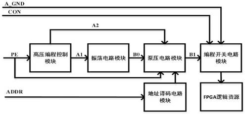
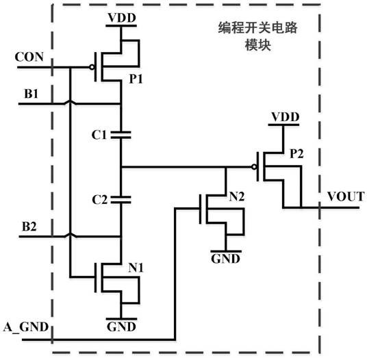
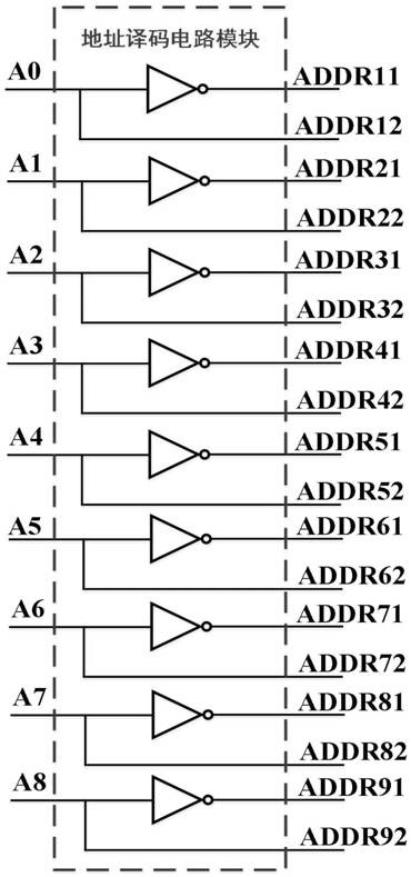
[0026] For the novel FPGA structure that the present invention designs, comprise address decoding circuit module, as image 3 As shown, it includes 9 inverters, and the output address of the decoding circuit is connected to the pumping circuit to control the high voltage output of the pumping circuit. Such as Figure 4 Shown is the overall implementation diagram of this design. Among them, the logic resources of the entire FPGA are divided into 9 power domains, namely BLOCK1, BLOCK2, BLOCK3, BLOCK4, BLOCK5, BLOCK6, BLOCK7, BLOCK8, and BLOCK9. The power on and off of each power domain is controlled by 9 programming switch circuits, and each programming switch circuit contains two anti-fuse devices to be programmed, which are ...


PUM


Abstract

The invention provides a novel FPGA structure of a power gating technology based on anti-fuse device control. Through the design of power gating, the objects of improving the chip yield, reducing the manufacturing cost of an FPGA chip and reducing the static power consumption of the FPGA are achieved. The on and off of a power switch device in the power gating technology are controlled by adopting an anti-fuse circuit. The control circuit has the advantages that the power-on and power-off sequence is controllable, and the yield of chips is improved.

Description

technical field [0001] The present invention relates to integrated circuit technology, and more specifically relates to a novel FPGA structure design based on power gating technology controlled by an antifuse device. Background technique [0002] The advancement of science and technology has continuously promoted the rapid development of my country's semiconductor industry. Field Programmable Gate Array (Field Programmable Gate Array, FPGA), as a branch of semiconductor devices, has gradually evolved into the core device of digital systems, and has been widely used in industrial control, automotive electronics, communications, aerospace, prototype verification and other fields. [0003] In the field of semiconductors, integrated circuit manufacturing technology has entered the era of nanotechnology. After the process size of semiconductor devices is lower than 90nm, static power consumption accounts for an increasing proportion of the total power consumption of FPGA. Power c...

Claims


Application Information

Patent Timeline
Patent Type & Authority Applications(China)
IPC IPC(8): G06F30/39
CPCG06F30/39Y02D10/00
Inventor 廖永波邹佳瑞李平冯轲刘玉婷徐璐刘仰猛侯伶俐熊宣淋
Owner UNIV OF ELECTRONICS SCI & TECH OF CHINA
Why Eureka
Try Eureka