Lead frame for diode forming, diode and manufacturing method of diode

A lead frame and diode technology, used in semiconductor/solid-state device manufacturing, electrical components, electrical solid-state devices, etc., can solve the problems of many processes, increase the number of lead frames, and high costs, reduce glue overflow gaps, and improve molding efficiency. The effect of good cost advantage

Pending Publication Date: 2021-06-25
众联慧合(天津)电子有限公司
View PDF0 Cites 0 Cited by
  • Summary
  • Abstract
  • Description
  • Claims
  • Application Information

AI Technical Summary

Problems solved by technology

[0004] The connecting sheet welding structure generally needs to manufacture the lead frame with the connecting sheet first, and then punch one or several connecting sheets from the frame at a time, and then absorb and place the punched connecting sheet on the chip lead frame for welding. The size of a single diode is small, and it is difficult to absorb and weld; the wire bonding structure requires gold wire or other metal wires, and it is not suitable to pass a large current; the double lead frame welding structure needs to increase the number of lead frames, and graphite boat welding can ensure Welder quality
Relatively speaking, the above three structures all have the problems of low efficiency and high cost
[0005] As far as the diode with the connecting piece welding structure is concerned, its processing needs to be completed on two pieces of profile frame, which requires many procedures and high cost; in order to facilitate the injection molding of the subsequent packaging shell, a special area is usually reserved on the lead frame as a ring. The special channel for epoxy resin injection molding will increase the area required for a single chip lead unit, thereby reducing the number of single chip lead units arranged on a frame profile, resulting in a low output rate of the profile and increasing the cost for the enterprise

Method used


Image

  • Lead frame for diode forming, diode and manufacturing method of diode
  • Lead frame for diode forming, diode and manufacturing method of diode
  • Lead frame for diode forming, diode and manufacturing method of diode

Examples


Embodiment Construction

[0039] Embodiments of the present invention are described in further detail below in conjunction with the accompanying drawings:

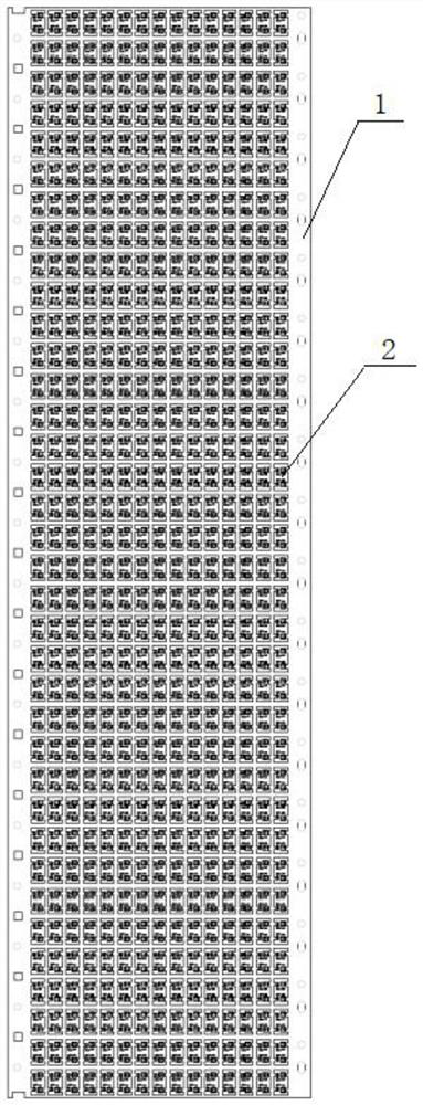
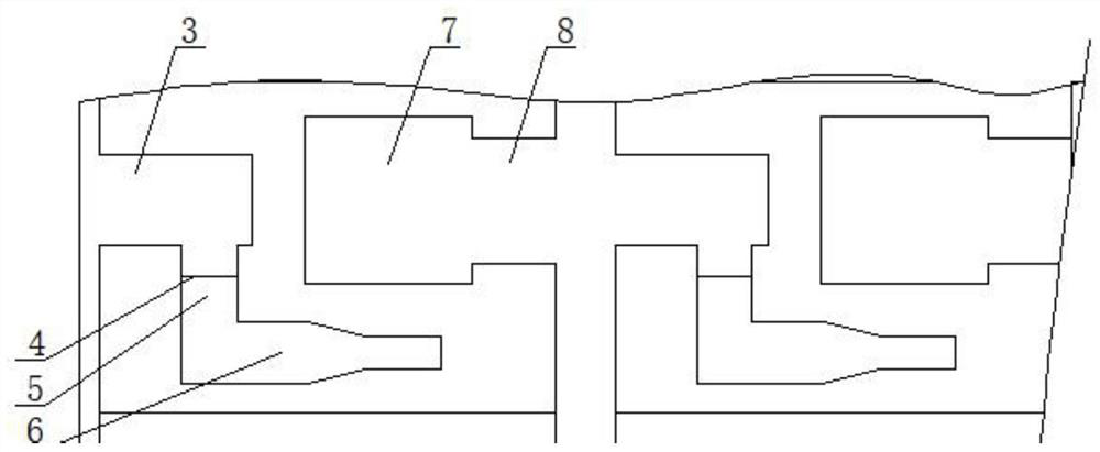
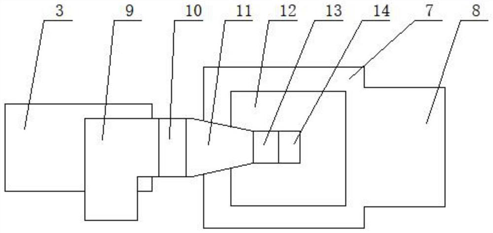
[0040] A lead frame for diode molding, including a profile 1, the innovation of which is that several diode frame units 2 are evenly spaced on the profile, and one or two diode frame units are arranged on each of the diode frame units. Diode molding bodies, such as figure 2As shown, a diode forming body is arranged in the diode frame, and each of the diode forming bodies is composed of a first pin 3, a second pin 8, a chip support piece 7 and a lead pole piece. The left and right sides of the frame of the diode frame unit are relatively provided with a first pin and a second pin integrated with the profile, and an L-shaped lead pole piece is integrally formed on the lower side of the first pin to the right. The L-shaped lead pole piece is composed of a connecting piece part 5 arranged perpendicularly to the first pin and a lead pole piece part 6 ...


PUM


Abstract

The invention relates to a lead frame for diode forming. The lead frame comprises a section bar, wherein a plurality of diode frame units are uniformly distributed on the section bar at intervals, one or two diode forming bodies are arranged in each diode frame unit, each diode forming body is composed of a first pin, a second pin, a chip supporting piece and a lead pole piece. The invention further relates to a diode. The diode is composed of a diode body and a packaging body packaged outside the diode body, wherein the diode body is formed by processing a diode forming body and a diode chip. The invention further relates to a manufacturing method of the diode. The manufacturing method comprises the steps of welding forming of the diode body and packaging of the packaging body outside the diode body. The lead frame of the invention has the advantages of scientific and reasonable design, high arrangement density, conservation of section bars, reduction in diode processing cost, convenient operation and easy realization.

Description

technical field [0001] The invention relates to a diode and its processing technology, in particular to a lead frame for forming a diode, a diode formed by using the lead frame and a manufacturing method. Background technique [0002] With the advancement of electronic semiconductor technology, diodes have developed from axial plug-in type diodes to bent-foot type SMD diodes, and then to flat-foot type SMD diodes. Electronic products are gradually developing towards miniaturization. In recent years, the ultra-thin flat-pin SMD diodes have exploded and gradually replaced traditional diodes. [0003] At present, there are mainly three types of packaging and welding structures for flat-foot diodes on the market, which are clip bonding, wire bonding and double leadframe welding. structure is the most widely used. [0004] The connecting sheet welding structure generally needs to manufacture the lead frame with the connecting sheet first, and then one or several connecting shee...

Claims


Application Information

Patent Timeline
Patent Type & Authority Applications(China)
IPC IPC(8): H01L23/495H01L29/861H01L21/48H01L21/60H01L21/329
CPCH01L23/4952H01L23/49541H01L29/861H01L29/6609H01L21/4825H01L24/85H01L2224/85986H01L2224/40245H01L2224/97
Inventor 孙丽
Owner 众联慧合(天津)电子有限公司
Why Eureka
Try Eureka