

BPSK modulation circuit based on low-power-consumption backscattering amplification tag and method thereof
A technology of backscattering and modulating circuits, applied in the field of wireless communication, can solve the problems of increased circuit complexity and increased power consumption, and achieve the effect of simple circuit implementation
- Summary
- Abstract
- Description
- Claims
- Application Information
AI Technical Summary
Problems solved by technology
Method used
Image

Examples
Embodiment 1
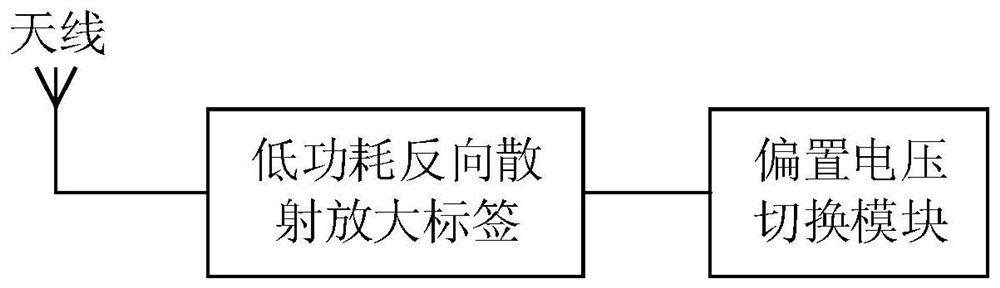
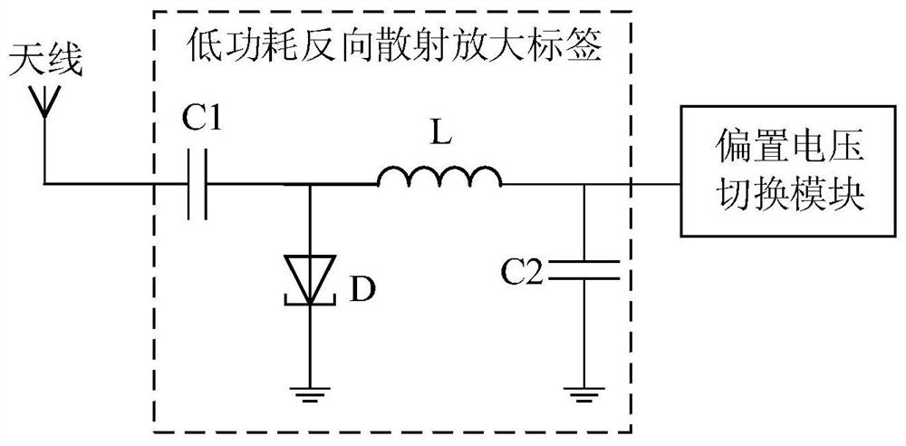
[0050] See figure 1 , figure 1 It is a schematic structural diagram of a BPSK modulation circuit based on a low-power backscatter amplification tag provided by an embodiment of the present invention. This embodiment proposes a BPSK modulation circuit based on a low-power backscatter amplification tag, including an antenna, a low-power backscatter amplification tag, and a bias voltage switching module.
[0051]Specifically, the BPSK modulation circuit of this embodiment includes a low-power backscattering amplification tag, a bias voltage switching module, and an antenna. Specifically, the function of the bias voltage switching module is to provide different bias voltages to control different bias voltages. The voltage supplies power to the low-power backscatter amplification tag; the function of the low-power backscatter amplification tag is to amplify and scatter the incident excitation signal with low power consumption. The specific bias voltage switching module enables the...
Embodiment 2
[0062] On the basis of the first embodiment above, please refer to Figure 4 , Figure 4 It is a schematic flowchart of a BPSK modulation method based on a low-power backscatter amplification tag provided by an embodiment of the present invention. This embodiment proposes a BPSK modulation method based on a low-power backscatter amplification tag, which is implemented based on the BPSK modulation circuit based on a low-power backscatter amplification tag described in Embodiment 1, and specifically includes the following steps:
[0063] Step 1. The bias voltage switching module provides several bias voltages.
[0064] Specifically, the bias voltage switching module of this embodiment outputs several different bias voltages through the DAC module of the single-chip microcomputer, so as to supply power to the low-power backscatter amplification tag under different bias voltages.
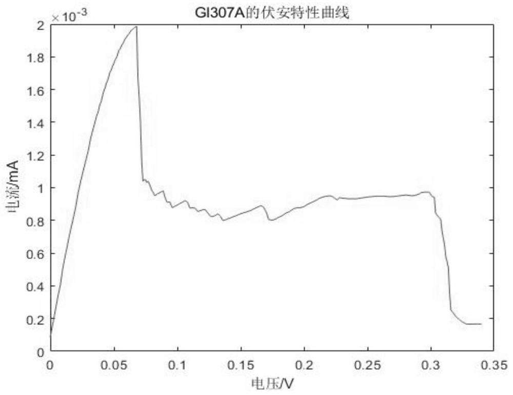
[0065] Step 2. Measure the low-power backscatter amplification tags under several bias voltages to...
PUM
 Abstract
Description
Claims
Application Information