
Cutting device for chip wafer processing

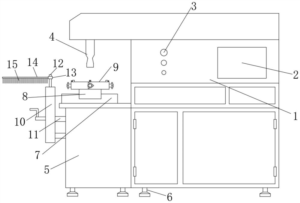
A cutting device and wafer technology, applied in metal processing, auxiliary devices, metal processing equipment, etc., can solve the problem of affecting chip wafer cutting processing, debris easily entering the next chip wafer, affecting cutting work, etc. question

Active Publication Date: 2021-07-02
深圳市尚鼎芯科技有限公司
View PDF14 Cites 4 Cited by
  • Summary
  • Abstract
  • Description
  • Claims
  • Application Information

AI Technical Summary

Problems solved by technology

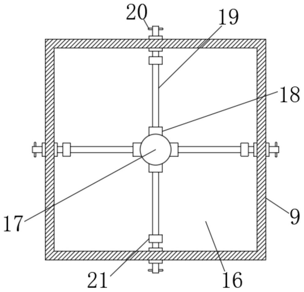
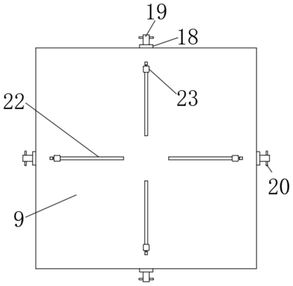
[0002] Wafer refers to the silicon wafer used to make silicon semiconductor circuits. Its raw material is silicon. High-purity polysilicon is dissolved and mixed with silicon crystal seeds, and then slowly pulled out to form cylindrical monocrystalline silicon. After grinding, polishing, and slicing, silicon wafers are formed, that is, wafers. During the processing of chip wafers, laser devices are often used to divide and cut the chip wafers. Therefore, before cutting, the chip wafers need to be The circle is fixed, and the traditional fixing structure mainly fixes the edge of the chip wafer through the rubber pad, and after the rubber pad and the chip wafer are in contact with each other, they will groove inward, so that the upper and lower sides are stuck on the chip. On the edge of the wafer, when the rubber pad is relatively thick, the area stuck on the edge of the chip wafer is relatively large, which is likely to affect the cutting process of the chip wafer position, and after the traditional laser cutting is completed, there are parts on the workbench Debris, the traditional dicing device does not have a cleaning structure, which makes it easy for these debris to enter the next chip wafer to be cut, affecting the cutting work

Method used


Image

  • Cutting device for chip wafer processing
  • Cutting device for chip wafer processing
  • Cutting device for chip wafer processing

Examples


Embodiment Construction

[0024] In order to make the technical means, creative features, goals and effects achieved by the present invention easy to understand, the present invention will be further described below in conjunction with specific embodiments.

[0025] In the description of the present invention, it should be noted that the terms "upper", "lower", "inner", "outer", "front end", "rear end", "both ends", "one end", "another end" The orientation or positional relationship indicated by etc. is based on the orientation or positional relationship shown in the drawings, and is only for the convenience of describing the present invention and simplifying the description, rather than indicating or implying that the referred device or element must have a specific orientation, use a specific Azimuth configuration and operation, therefore, should not be construed as limiting the invention. In addition, the terms "first" and "second" are used for descriptive purposes only, and should not be understood ...


PUM


Abstract

The invention discloses a cutting device for chip wafer processing. The cutting device comprises a main machine body, a display screen is arranged on the main machine body, a side machine body is arranged on the side face of the main machine body, a transverse moving body is arranged on the side machine body, and a vertical moving body is movably installed on the transverse moving body. A workbench is arranged on the vertical moving body, a laser cutting head is arranged at the position, above the workbench, of the main machine body, a first internal storage bin is arranged in the workbench, and a middle mounting body is arranged in the middle of the first internal storage bin. The cutting device for chip wafer processing belongs to the field of chip wafer processing. The chip wafer is fixed through the arranged upper clamping body and other structures, the situation that a rubber pad occupies an overlarge area of the edge position and influences processing is prevented, and the workbench is convenient to clean through the arranged upper brush plate and other structures, and the chippings are prevented from influencing the processing of the next chip wafer.

Description

technical field [0001] The invention relates to the field of cutting devices, in particular to a cutting device for chip wafer processing. Background technique [0002] Wafer refers to the silicon wafer used to make silicon semiconductor circuits. Its raw material is silicon. High-purity polysilicon is dissolved and mixed with silicon crystal seeds, and then slowly pulled out to form cylindrical monocrystalline silicon. After grinding, polishing, and slicing, silicon wafers are formed, that is, wafers. During the processing of chip wafers, laser devices are often used to divide and cut the chip wafers. Therefore, before cutting, the chip wafers need to be The circle is fixed, and the traditional fixing structure mainly fixes the edge of the chip wafer through the rubber pad, and after the rubber pad and the chip wafer are in contact with each other, they will groove inward, so that the upper and lower sides are stuck on the chip. On the edge of the wafer, when the rubber pa...

Claims


Application Information

Patent Timeline
Patent Type & Authority Applications(China)
IPC IPC(8): B23K26/38B23K26/70B23K37/04B23K26/16H01L21/304H01L21/687
CPCB23K26/38B23K26/702B23K37/04B23K26/16H01L21/304H01L21/68785B23K2101/40B23K2103/56
Inventor 刘道国
Owner 深圳市尚鼎芯科技有限公司
Learn More