Method for testing density distribution of recombination current on surface of double-sided symmetrical passivated silicon wafer

A test method and technology on the surface of silicon wafers, applied in the field of solar cells, which can solve the problems that areas cannot be separated for evaluation, and the distribution of composite current density cannot be obtained.

Active Publication Date: 2021-07-06
CSI CELLS CO LTD +1
View PDF4 Cites 4 Cited by
  • Summary
  • Abstract
  • Description
  • Claims
  • Application Information

AI Technical Summary

Problems solved by technology

This has caused some limitations: first, the composite current density distribution on the entire surface of the sample cannot be obtained, and second, some defects are much smaller than the WCT-120 sensor area, and this part of the area cannot be isolated for evaluation

Method used


Image

  • Method for testing density distribution of recombination current on surface of double-sided symmetrical passivated silicon wafer
  • Method for testing density distribution of recombination current on surface of double-sided symmetrical passivated silicon wafer
  • Method for testing density distribution of recombination current on surface of double-sided symmetrical passivated silicon wafer

Examples


Embodiment 1

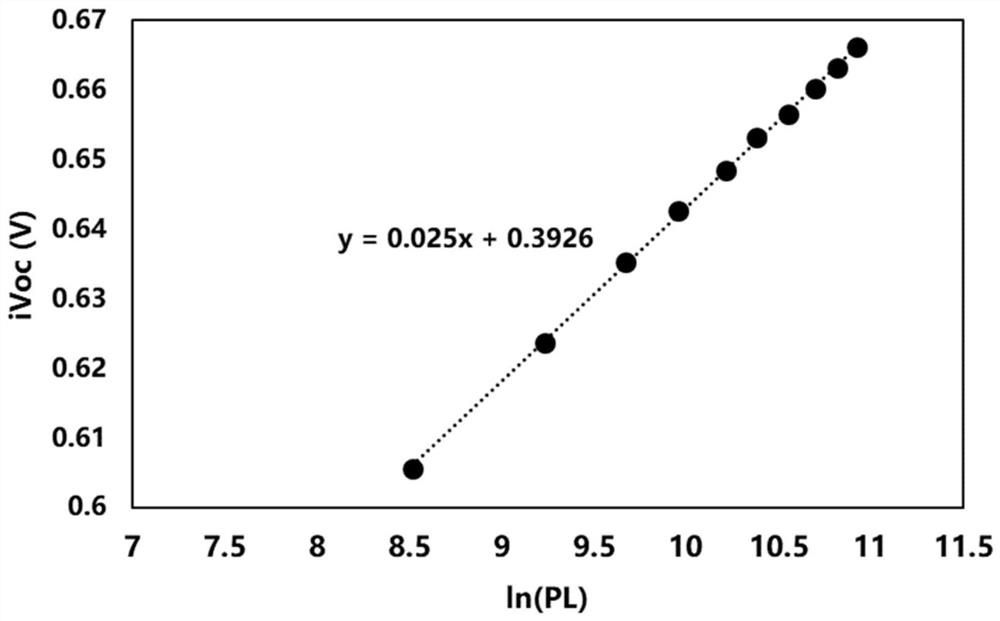
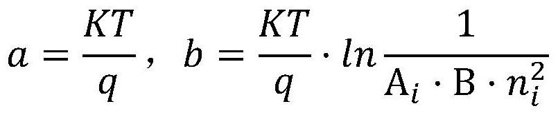
[0054] This embodiment provides a method for testing the recombination current density distribution on the surface of a double-sided symmetrical passivated silicon wafer.

[0055] Sample preparation:

[0056] 1. To select a P-type silicon chip, the resistivity is required to be greater than 10Ω.cm, and the measured resistivity of the silicon chip is ρ=25.4Ω·cm. The calculated bulk doping concentration NA is 5.3×10 14 cm -3 ;

[0057] 2. Adopt the conventional texture-making process of the production line to form texture on both surfaces of the silicon wafer;

[0058] 3. Adopt the conventional diffusion process of the production line to form diffusion surfaces on both surfaces of the silicon wafer;

[0059] 4. Prepare a HF solution with a mass concentration of 8%, and remove the phosphosilicate glass formed by diffusion;

[0060] 5. Silicon nitride film is coated on both sides to form a protective layer and passivate the surface of the sample;

[0061] 6. After sintering i...

Embodiment 2

[0084] This embodiment provides a method for testing the recombination current density distribution on the surface of a double-sided symmetrical passivated silicon wafer.

[0085] Sample preparation:

[0086] 1. Select N-type silicon wafers, the resistivity is required to be greater than 10Ω.cm, and the measured resistivity of the silicon wafers is ρ=7.1Ω·cm. The calculated bulk doping concentration NA is 6.51×10 14 cm -3 ;

[0087] 2. Adopt the conventional texture-making process of the production line to form texture on both surfaces of the silicon wafer;

[0088] 3. Adopt the conventional diffusion process of the production line to form diffusion surfaces on both surfaces of the silicon wafer, and anneal the bulk material at the same time to improve the bulk life of the material;

[0089] 4. Prepare a KOH solution with a mass concentration of 7.2%, polish the surface of the silicon wafer, and remove the pn junction diffused on the surface;

[0090] 5. Aluminum oxide pla...


PUM

PropertyMeasurementUnit
electrical resistivityaaaaaaaaaa
thicknessaaaaaaaaaa

Abstract

The invention provides a method for testing density distribution of recombination current on the surface of a double-sided symmetrical passivated silicon wafer. The testing method comprises the following steps: preparing a double-sided symmetrical passivated silicon wafer, and testing the thickness and the average reflectivity; under a series of illumination conditions with different intensities, testing excess carrier concentration [delta]n and average luminous intensity PL of a to-be-tested area of a double-sided symmetric passivation silicon wafer, and calculating an iVoC value according to [delta]n; establishing a linear relational expression iVoc=a*ln(PL)+b between the iVoc and the ln (PL); and illuminating the double-sided symmetric passivated silicon wafer, testing the luminous intensity PLij of any region, and calculating the recombination current density distribution J0ij of the surface of the double-sided symmetric passivated silicon wafer according to the relational expression iVOCij =a.ln (PLij)+b and the PLij value. The testing method provided by the invention has the resolution far higher than that of a minority carrier lifetime tester, and can obtain the recombination current density distribution on the whole surface of the double-surface symmetrical passivation silicon wafer.

Description

technical field [0001] The invention belongs to the technical field of solar cells, and in particular relates to a method for testing the recombination current density distribution on the surface of a double-sided symmetrical passivated silicon wafer. Background technique [0002] Photoluminescence (PL) detection equipment is the main test equipment to characterize the ability of solar cells to recombine carriers. Its working principle is to irradiate the sample with a certain intensity of laser light, the sample absorbs photons and generates electron-hole pairs, and the electron-hole recombination The light of a specific wavelength is directly recombined and emitted, and the light of the specific wavelength is collected by the detector and converted into a numerical matrix according to its intensity to form an image. If there is a recombination center in the solar cell, such as metal impurities, dislocations, etc., the electrons and holes will not recombine directly but wil...

Claims


Application Information

Patent Timeline
Patent Type & Authority Applications(China)
IPC IPC(8): G01N21/64G01R31/26
CPCG01N21/6489G01R31/2648G01R31/2601
Inventor 李硕杨慧邓伟伟蒋方丹
Owner CSI CELLS CO LTD
Why Eureka
Try Eureka