Electrical element manufacturing device and method for semiconductor device production

A technology for electrical components and manufacturing devices, which is applied in semiconductor/solid-state device manufacturing, electrical components, circuits, etc., and can solve problems such as thick photoresist and high viscosity of photoresist

Active Publication Date: 2021-07-06
江苏振宁半导体研究院有限公司
View PDF4 Cites 3 Cited by
  • Summary
  • Abstract
  • Description
  • Claims
  • Application Information

AI Technical Summary

Problems solved by technology

[0004] The purpose of the present invention is to solve the problem that in the prior art, fine dust is easy to appear around, and during the conveying process of the photoresist, the temperature is too low to cause the

Method used


Image

  • Electrical element manufacturing device and method for semiconductor device production
  • Electrical element manufacturing device and method for semiconductor device production
  • Electrical element manufacturing device and method for semiconductor device production

Examples


Embodiment 1

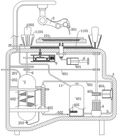
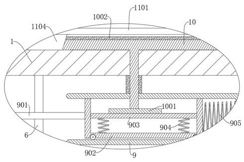
[0030] refer to Figure 1-6 , an electrical component manufacturing device for semiconductor device production, including a box body 1 and a processed product 101, and also includes: a storage tank 2 and a water tank 401, both located in the box body 1; a mechanical arm 3, located at the top of the box body 1; a coating head 301 , connected to the output end of the mechanical arm 3, the processed product 101 is smeared by the smear head 301, and the smear head 301 and the storage tank 2 are transported through the discharge pipe 202; Hot water for heat preservation; the top of the box body 1 is provided with an electrostatic adsorption body 1003, and the bottom of the adsorption body 1003 is covered with a dust receiving cylinder 1104; the nozzle 1105 is connected to the inner wall of the dust receiving cylinder 1104, and the nozzle 1105 is connected to the top of the water tank 401. The water vapor in the water tank 401 is used for dust reduction; wherein, the processed produ...

Embodiment 2

[0033] refer to Figure 1-6 , on the basis of Example 1, further,

[0034]A motor 4, a heat conduction tank 402 and a first piston assembly 404 are also provided in the box body 1. The output end of the motor 4 is connected to a crankshaft 403, and the crankshaft 403 is rotationally connected to the first piston assembly 404. Between the water tank 401 and the first piston assembly 404 The first piston assembly 404 is connected to the top of the heat conducting tank 402 through the second pipeline 501, the bottom of the heat conducting tank 402 is connected to the water tank 401 through the third pipeline 502, and the first pipeline 5 1. Both the second pipeline 501 and the third pipeline 502 are provided with check valves, the heat conduction tank 402 is made of heat conduction material, the discharge pipe 202 is wound on the surface of the heat conduction tank 402, and the water tank 401 is provided with a heating wire 405.

[0035] This embodiment discloses the specific pr...

Embodiment 3

[0038] refer to Figure 1-6 , on the basis of Example 2, further,

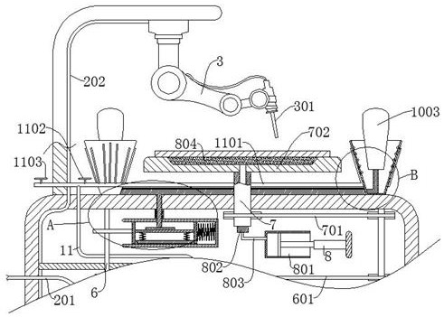
[0039] The top of the box body 1 is rotatably connected with a rotating rod 7, and the top of the rotating rod 7 is fixedly connected with a workbench 702. The workbench 702 is provided with a suction cup 804, and the processed product 101 is placed on the suction cup 804. The rotating rod 7 and the output end of the motor 4 pass through The second belt 701 is connected.

[0040] The casing 1 is provided with a cylinder 8 and a second piston assembly 801, the output end of the cylinder 8 is connected with the second piston assembly 801, the second piston assembly 801 is connected with the suction cup 804 through the sixth pipeline 803, and the sixth pipeline 803 is provided with a swivel joint 802, and the swivel joint 802 is connected to the bottom of the swivel rod 7.

[0041] This embodiment discloses the fixing method of the processed product 101. The processed product 101 is placed on the suction cup 80...


PUM


Abstract

The invention discloses an electrical element manufacturing device and method for semiconductor device production, and belongs to the technical field of semiconductor manufacturing. The electrical element manufacturing device for semiconductor device production comprises: a box body and a processed product; a storage tank and a water box both located in the box body; a mechanical arm located at the top of the box body; and a smearing head connected to the output end of the mechanical arm, wherein the the processed product is smeared through the smearing head, conveying is conducted between the smearing head and the storage tank through a discharging pipe, the discharging pipe is subjected to heat preservation through hot water in the water box in the conveying process, and an adsorption body with static electricity is arranged at the top of the box body. Compared with an existing electrical element manufacturing device for semiconductor device production in the market, the electrical element manufacturing device for semiconductor device production can use water vapor generated by heat preservation of a photoresist to carry out dust fall after coating is completed.

Description

technical field [0001] The invention relates to the technical field of semiconductor manufacturing, in particular to an electrical component manufacturing device and a manufacturing method for semiconductor device production. Background technique [0002] A semiconductor device is an electronic device whose conductivity is between a good conductor and an insulator. It uses the special electrical characteristics of semiconductor materials to complete specific functions. It can be used to generate, control, receive, transform, amplify signals and perform energy conversion. The semiconductor of semiconductor devices The material is silicon, germanium or gallium arsenide, which can be used as rectifiers, oscillators, light emitters, amplifiers, photometers and other equipment. [0003] In some products made by semiconductor devices, such as the manufacturing process of chips, it is necessary to apply a layer of photoresist on the surface, and then process it. When applying photo...

Claims


Application Information

Patent Timeline
IPC IPC(8): H01L21/67G03F7/16
CPCG03F7/16H01L21/6715
Inventor 姬煜
Owner 江苏振宁半导体研究院有限公司
Why Eureka
Try Eureka