Erasable printing technology for plasmon colors
A plasmonic and color technology, applied in the field of erasable printing technology of plasmonic color, to achieve the effect of high-efficiency color printing and simple operation requirements
- Summary
- Abstract
- Description
- Claims
- Application Information
AI Technical Summary
Problems solved by technology
Method used
Image
Examples
Embodiment 1
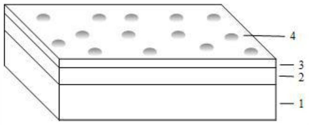
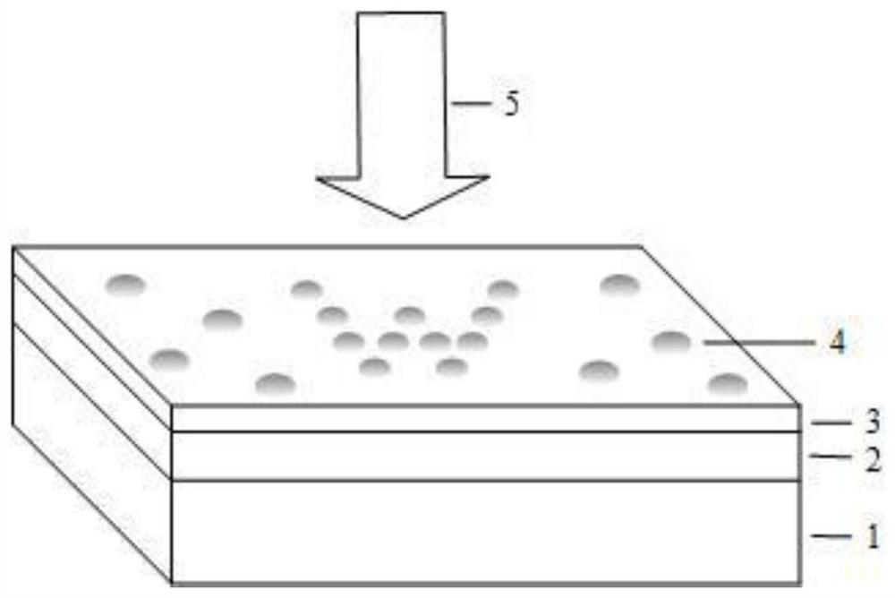
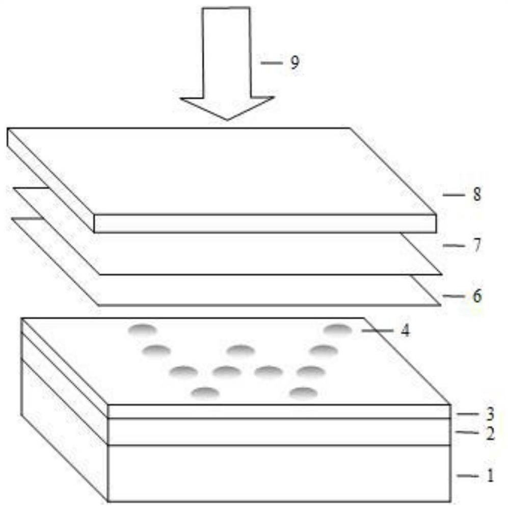
[0029] Figure 1-4 It is a schematic diagram of the steps of the erasable printing technology of plasmonic color according to the present invention. 100nm thick reflective metal Ag was deposited on the glass slide; 30nm thick SiO was deposited on the surface of Ag metal by plasma-enhanced chemical vapor deposition (PECVD) 2 Dielectric, as the spacer layer; deposit 10nm thick Ag on the surface of the spacer layer, such as figure 1 As shown; use a 405nm laser with a power of 100% and a burning time of 6ms to scan the surface of metal Ag, and write the letter "W", such as figure 2 shown. The Ag was observed to turn green under the light microscope, and the SEM image showed that the Ag nanoparticles were reduced in size, such as Figure 5 As shown; lay a layer of graphite-coated aluminum foil on the surface of the scanned sample with a thickness of 4 μm, and then cover it with transparent glass (the thickness of the transparent glass is 0.5 mm) as a transparent solid layer; us...
PUM
| Property | Measurement | Unit |
|---|---|---|
| thickness | aaaaa | aaaaa |
| thickness | aaaaa | aaaaa |
| thickness | aaaaa | aaaaa |
Abstract
Description
Claims
Application Information


