Growth method of light-emitting diode epitaxial wafer

A technology for light emitting diodes and a growth method, which is applied to the growth field of light emitting diode epitaxial wafers, and can solve the problems of decreasing internal quantum efficiency, lattice mismatch, affecting the luminous efficiency of LEDs, etc.

Active Publication Date: 2021-07-13
HC SEMITEK SUZHOU
View PDF4 Cites 0 Cited by
  • Summary
  • Abstract
  • Description
  • Claims
  • Application Information

AI Technical Summary

Problems solved by technology

However, there is a large lattice mismatch between the InGaN layer and the GaN layer, resulting in a large compressive stress between the InGaN layer and the GaN layer
Compressive stress will generate a piezoelectric polarization electric f

Method used


Image

  • Growth method of light-emitting diode epitaxial wafer
  • Growth method of light-emitting diode epitaxial wafer
  • Growth method of light-emitting diode epitaxial wafer

Examples


Embodiment Construction

[0027] In order to make the purpose, technical solution and advantages of the present disclosure clearer, the implementation manners of the present disclosure will be further described in detail below in conjunction with the accompanying drawings.

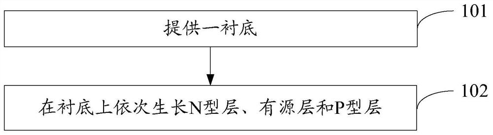
[0028] figure 1 It is a flow chart of a method for growing a light-emitting diode epitaxial wafer provided by an embodiment of the present disclosure, as shown in figure 1 As shown, the growth method includes:

[0029] Step 101, providing a substrate.

[0030] Wherein, the substrate may be a sapphire substrate.

[0031] Step 102 , growing an N-type layer, an active layer and a P-type layer sequentially on the substrate.

[0032] Wherein, the active layer includes a plurality of alternately grown InGaN quantum well layers and GaN quantum barrier layers.

[0033] Exemplarily, in step 102, when growing each InGaN quantum well layer of the active layer, ammonia gas is injected into the reaction chamber at a low speed, and the flow ...


PUM

PropertyMeasurementUnit
Thicknessaaaaaaaaaa
Growth temperatureaaaaaaaaaa

Abstract

The invention provides a growth method of a light-emitting diode epitaxial wafer, and belongs to the technical field of semiconductors. The growth method comprises the following steps: providing a substrate; and sequentially growing an N-type layer, an active layer and a P-type layer on the substrate, wherein the active layer comprises a plurality of InGaN quantum well layers and GaN quantum barrier layers which are periodically and alternately grown, wherein when each InGaN quantum well layer of the active layer grows, ammonia gas is introduced into the reaction chamber at a low speed, and the flow of the ammonia gas introduced into the reaction chamber is controlled to be gradually increased and then gradually reduced. According to the growth method, the formation of quantum dots in the InGaN quantum well layer can be increased, so that the probability of non-radiative recombination of electrons and holes is greatly reduced, and the internal quantum luminous efficiency of an LED can be improved.

Description

technical field [0001] The present disclosure relates to the technical field of semiconductors, in particular to a method for growing an epitaxial wafer of a light emitting diode. Background technique [0002] A light-emitting diode (English: Light Emitting Diode, referred to as: LED) is a semiconductor electronic component that can emit light. As an efficient, environmentally friendly and green new solid-state lighting source, LED is a new generation of light source with broad prospects, and is being rapidly and widely used in traffic lights, car interior and exterior lights, urban landscape lighting, indoor and outdoor display screens and small-pitch displays. screen and other fields. [0003] The epitaxial wafer is the primary product in the LED manufacturing process. In related technologies, an LED epitaxial wafer includes a substrate and an N-type layer, an active layer and a P-type layer stacked on the substrate in sequence. Wherein, the N-type layer is used to prov...

Claims


Application Information

Patent Timeline
IPC IPC(8): H01L33/00H01L33/06
CPCH01L33/007H01L33/06
Inventor 姚振从颖董彬忠李鹏
Owner HC SEMITEK SUZHOU
Why Eureka
Try Eureka