
Silicon-based liquid crystal panel and design method and preparation method thereof

A silicon-based liquid crystal and design method technology, applied in design optimization/simulation, special data processing applications, optics, etc., can solve problems such as high manufacturing cost, low light utilization rate of silicon-based liquid crystal panels, inconsistent reflectivity, etc., to achieve a wide range of Effects of economic value, improvement of light utilization rate, and expansion of scope of application

Pending Publication Date: 2021-07-20
西安中科微星光电科技有限公司
View PDF3 Cites 4 Cited by
  • Summary
  • Abstract
  • Description
  • Claims
  • Application Information

AI Technical Summary

Problems solved by technology

The upper substrate of the existing liquid crystal on silicon panel is mainly ITO glass. The thickness of the ITO glass and the ITO material on the top lead to the difference in transmittance, and the transmittance is mainly between 75% and 90%. The lower substrate is mainly a silicon wafer. The difference between the CMOS circuit on the silicon wafer and the reflective aluminum layer will lead to inconsistent reflectivity, and the reflectivity is mainly between 70% and 95%. Generally speaking, the existing liquid crystal on silicon panel The light utilization rate is between 50% and 85%, with a large difference
The light utilization rate of the existing liquid crystal on silicon panel is affected by the pixel size and pixel gap on the silicon substrate, but it is mainly limited by the manufacturing process capability of the silicon substrate and the financial pressure of developing the mask plate.
[0003] That is to say, the manufacturing process capability of the silicon substrate of the existing liquid crystal on silicon panel is insufficient, and the manufacturing cost is high, which leads to the inability to obtain a liquid crystal on silicon panel with high light utilization rate while spending a relatively high production cost
Moreover, due to the low light utilization efficiency of the existing liquid crystal on silicon panel, its corresponding scope of application is relatively limited.

Method used


Image

  • Silicon-based liquid crystal panel and design method and preparation method thereof
  • Silicon-based liquid crystal panel and design method and preparation method thereof
  • Silicon-based liquid crystal panel and design method and preparation method thereof

Examples


Embodiment Construction

[0037] The following description serves to disclose the present invention to enable those skilled in the art to carry out the present invention. The preferred embodiments described below are only examples, and those skilled in the art can devise other obvious variations. The basic principles of the present invention defined in the following description can be applied to other embodiments, variations, improvements, equivalents and other technical solutions without departing from the spirit and scope of the present invention.

[0038] Those skilled in the art should understand that, in the disclosure of the present invention, the terms "vertical", "transverse", "upper", "lower", "front", "rear", "left", "right", The orientations or positional relationships indicated by "vertical", "horizontal", "top", "bottom", "inner", "outer", etc. are based on the orientation or positional relationship shown in the drawings, which are only for the convenience of describing the present inventi...


PUM

PropertyMeasurementUnit
thicknessaaaaaaaaaa
reflectanceaaaaaaaaaa

Abstract

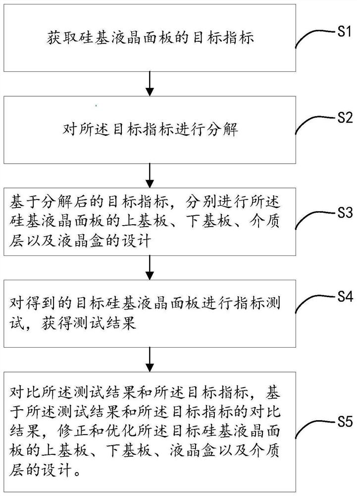
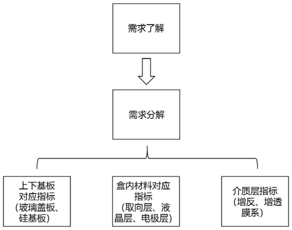
The invention relates to a silicon-based liquid crystal display panel and a design method and a preparation method thereof. an upper substrate, a lower substrate and a liquid crystal box of the silicon-based liquid crystal display panel are respectively designed by obtaining a target index of the silicon-based liquid crystal display panel and decomposing the target index, and finally an antireflection film is formed on the upper substrate through evaporation, the light utilization rate of the silicon-based liquid crystal panel is comprehensively and effectively improved in a mode of forming the high-reflection film on the lower substrate through evaporation, so that the light utilization rate of a product using the silicon-based liquid crystal panel is improved, and the application range of the silicon-based liquid crystal panel is favorably widened; according to the preparation method of the silicon-based liquid crystal panel, coating treatment is carried out before packaging of the silicon substrate, the structure of an existing silicon substrate does not need to be changed, the preparation method is simple and easy to implement, and the silicon-based liquid crystal panel with the higher light utilization rate can be obtained with the low production cost.

Description

technical field [0001] The invention relates to the technical field of silicon-based liquid crystal panel manufacturing, in particular to a silicon-based liquid crystal panel and a design method and a preparation method thereof. Background technique [0002] The light utilization efficiency of the existing LCOS wafer substrate (silicon substrate) is relatively low, ranging from 70% to 95%. The upper substrate of the existing liquid crystal on silicon panel is mainly ITO glass. The thickness of the ITO glass and the ITO material on the top lead to the difference in transmittance, and the transmittance is mainly between 75% and 90%. The lower substrate is mainly a silicon wafer. The difference between the CMOS circuit on the silicon wafer and the reflective aluminum layer will lead to inconsistent reflectivity, and the reflectivity is mainly between 70% and 95%. Generally speaking, the existing liquid crystal on silicon panel The light utilization rate is between 50% and 85%,...

Claims


Application Information

Patent Timeline
Patent Type & Authority Applications(China)
IPC IPC(8): G06F30/20G02F1/1333
CPCG06F30/20G02F1/1333
Inventor 夏高飞宇磊磊张宁峰王华高宇
Owner 西安中科微星光电科技有限公司
Learn More