Double-groove step buffer gate 4H-SiC metal semiconductor field effect transistor and modeling simulation method

A technology of metal semiconductors and field effect transistors, applied in semiconductor devices, transistors, special data processing applications, etc., can solve the problems of current density decrease and limit power density, etc., achieve power density improvement, increase saturation current density, and optimize electric field lines distribution effect

Inactive Publication Date: 2021-08-03
QINGDAO UNIV OF SCI & TECH
View PDF3 Cites 0 Cited by
  • Summary
  • Abstract
  • Description
  • Claims
  • Application Information

AI Technical Summary

Problems solved by technology

However, in the prior art, only a slight increase in drain current density or breakdown voltage was achieved, and even performance on the one hand had to be sacrificed in order to improve both, because there is a trade-off between current density and breakdown voltage. A mutual constraint relationship, which limits the effective improvement of power density
The prior art discloses a stepped buffer gate structure 4H-SiC MESFET (SBG 4H-SiC MESFET), which has outstanding breakdown characteristics but slightly lower current density

Method used


Image

  • Double-groove step buffer gate 4H-SiC metal semiconductor field effect transistor and modeling simulation method
  • Double-groove step buffer gate 4H-SiC metal semiconductor field effect transistor and modeling simulation method
  • Double-groove step buffer gate 4H-SiC metal semiconductor field effect transistor and modeling simulation method

Examples


Embodiment 1

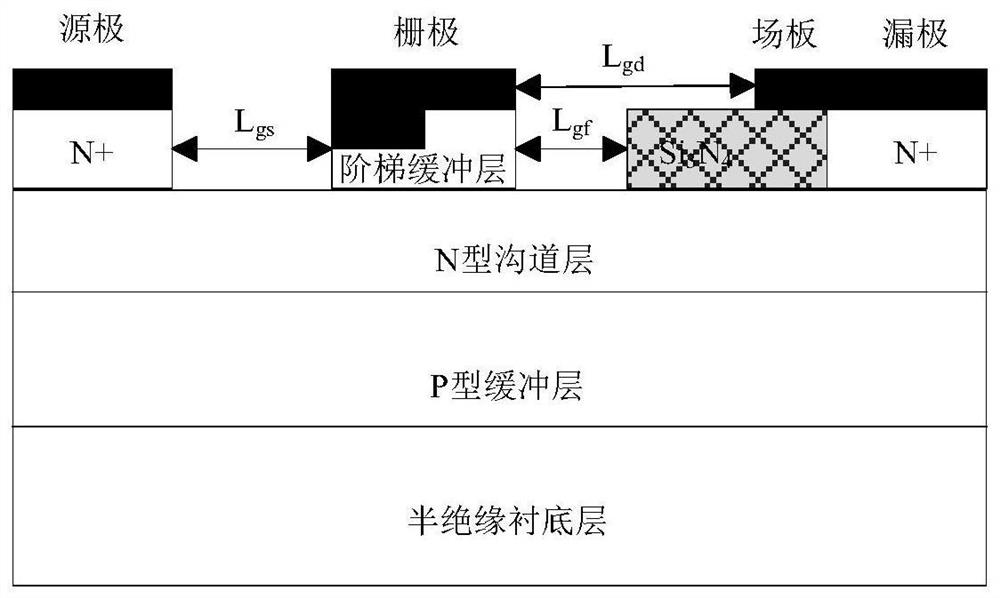
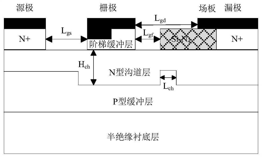
[0064] like figure 1 and figure 2 As shown, the schematic diagrams of the prior art (hereinafter referred to as SBG MESFET) and the present invention (hereinafter referred to as SBG-MRMESFET) are respectively. These two structures are composed of 4H-SiC semi-insulating substrate layer, P-type buffer layer, N-type channel layer, two heavily doped N-type cap layers and between the gate and N-type channel from bottom to top. The ladder buffer gate layer composition. The only difference between these two structures is that two grooves are introduced on top of the P-type buffer layer of the SBG-MR MESFET, i.e. the first groove is under the gate and the second groove is between the field plate and drain below the pole. The depth and length of the two grooves are the same, 0.15 μm and 1 μm, respectively. The length of the small pillar between the two grooves (L ch ) is 0.2 μm. For comparison, the parameter values ​​used in the simulations are equal and listed in Table 1.

[0...

Embodiment 2

[0087] In the present invention, the output characteristics of the SBG-MR 4H-SiC MESFET and the SBG4H-SiC MESFET will be simulated under the same structural parameters for comparison.

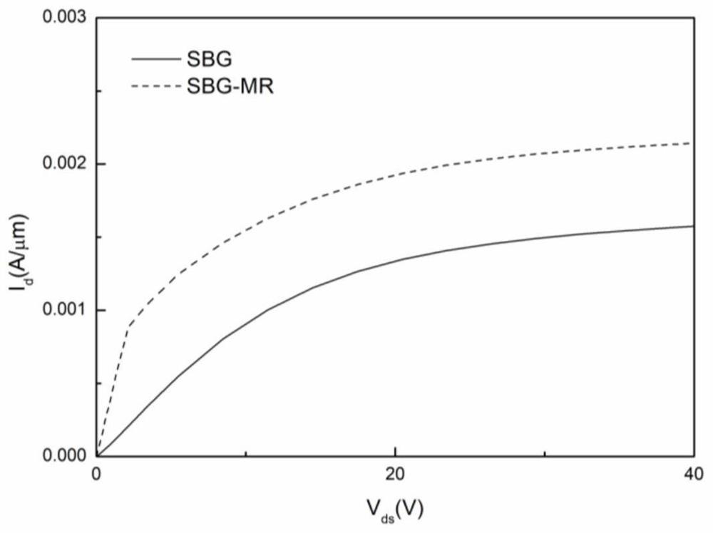
[0088] image 3 shows the V gs = 0V and V ds = Saturation drain current curve under the condition of 40V. It can be seen that the maximum saturated drain current density of the SBG4H-SiC MESFET is 0.0016A / μm, while that of the SBG-MR 4H-SiC MESFET is 0.0022A / μm, which is 37.5% higher than that of the SBG structure.

[0089] Figure 4(a) and Figure 4(b) depict the internal electron flow profiles of these two structures, and the current density of the SBG-MR structure marked in Figure 4(b) is significantly higher than that of the SBG structure in Figure 4(a) density. The reason for these differences is that the two grooves introduced by the p-buffer layer of the SBG-MR structure provide a wider channel, that is, a larger total channel cross-section. This means that the resistance of the SBG-M...


PUM

PropertyMeasurementUnit
lengthaaaaaaaaaa
lengthaaaaaaaaaa
thicknessaaaaaaaaaa

Abstract

The invention relates to a double-groove step buffer gate 4H-SiC metal semiconductor field effect transistor and a modeling simulation method, and belongs to the technical field of power semiconductor devices. The metal semiconductor field effect transistor comprises a 4H-SiC semi-insulating substrate layer, a P-type buffer layer, a first groove, a second groove and an N-type channel layer, a source cap layer and a drain cap layer are arranged on the upper end face of the N-type channel layer, and a step buffer gate layer is arranged between the gate and the upper surface of the N-type channel layer; a field plate is formed by extending a certain distance from the drain electrode to the grid electrode, and a passivation layer Si3N4 is arranged between the drain electrode and the grid electrode; the first groove and the second groove are formed in the top of the P-type buffer layer, the first groove is located below the grid electrode, and the second groove is located below the drain electrode cap layer and the field plate. According to the invention, the double grooves are introduced above the P-type buffer layer, so that the saturation current density is greatly improved; the distribution of electric field lines is optimized, and the breakdown voltage is increased by nearly 10%; and finally, the power density is greatly improved by 55%.

Description

technical field [0001] The invention relates to a double-groove stepped buffer gate 4H-SiC metal semiconductor field effect transistor and a modeling simulation method, belonging to the technical field of power semiconductor devices. Background technique [0002] Silicon carbide (SiC) has attracted extensive attention due to its excellent electrical properties such as wide bandgap, high saturation electron mobility, and high thermal conductivity. It has been widely used in environments with extreme high temperature, high power and high radiation. 4H-SiC-based MESFETs (4H-SiC MESFETs) occupy an extremely important position in high-power applications and have become a research hotspot in recent years. However, in the prior art, only a slight increase in drain current density or breakdown voltage was achieved, and even performance on the one hand had to be sacrificed in order to improve both, because there is a trade-off between current density and breakdown voltage. A mutual...

Claims


Application Information

Patent Timeline
Patent Type & Authority Applications(China)
IPC IPC(8): H01L29/812H01L29/06H01L29/10G06F30/367
CPCH01L29/812H01L29/0619H01L29/1029G06F30/367
Inventor 张现军李娜邱恒远游娜王明甲秦浩华覃庆良冯宇平孙绍华
Owner QINGDAO UNIV OF SCI & TECH
Why Eureka
Try Eureka