A kind of semiconductor device and its manufacturing method

A manufacturing method and semiconductor technology, applied in the fields of semiconductor/solid-state device manufacturing, electrical components, circuits, etc., can solve the problem that the deposition temperature of the metal layer cannot be too high, and achieve the effect of reducing the difficulty of deposition

Active Publication Date: 2021-09-24
SUZHOU HUNTERSUN ELECTRONICS CO LTD +1
View PDF9 Cites 0 Cited by
  • Summary
  • Abstract
  • Description
  • Claims
  • Application Information

AI Technical Summary

Problems solved by technology

[0003] In view of this, an embodiment of the present invention provides a semiconductor device and its manufacturing method to solve the problem that the deposition temperature of the metal layer produced by the existing metal lift-off process cannot be too high

Method used


Image

  • A kind of semiconductor device and its manufacturing method
  • A kind of semiconductor device and its manufacturing method
  • A kind of semiconductor device and its manufacturing method

Examples


Embodiment Construction

[0045] The following will clearly and completely describe the technical solutions in the embodiments of the present invention with reference to the accompanying drawings in the embodiments of the present invention. Obviously, the described embodiments are only part of the embodiments of the present invention, not all of them. Based on the embodiments of the present invention, all other embodiments obtained by persons of ordinary skill in the art without making creative efforts belong to the protection scope of the present invention.

[0046] An embodiment of the present invention provides a method for manufacturing a semiconductor device, such as Figure 4 As shown, the method includes:

[0047] S101: providing a substrate;

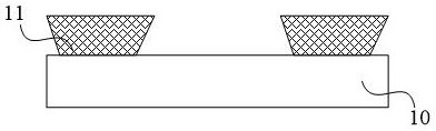
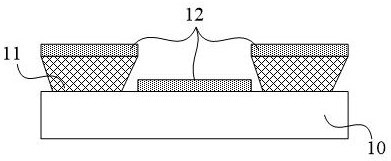
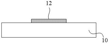
[0048] Such as Figure 5 As shown, in some embodiments of the present invention, the substrate 20 can be a semiconductor substrate, such as a silicon substrate, a silicon germanium substrate, etc., but in other embodiments of the present invention, the ...


PUM


Abstract

An embodiment of the present invention provides a semiconductor device and a manufacturing method thereof. The method includes: sequentially depositing a first mask layer and a second mask layer on a substrate, and performing a process on the first mask layer and the second mask layer. Etching to form a groove exposing the substrate, forming a metal layer on the substrate exposed by the groove and the second mask layer, and removing the first mask layer, the second mask layer and the second mask layer the metal layer on the substrate, leaving the metal layer on the substrate exposed by the recess. Since the first mask layer and the second mask layer are thin film layers fabricated on the substrate by a deposition process rather than a photoresist layer, even if the temperature of the subsequent deposition process for forming the metal layer is too high, it will not It affects the first mask layer and the second mask layer, that is, the first mask layer and the second mask layer formed by the deposition process do not require a high deposition temperature of the metal layer, thereby reducing the difficulty of depositing the metal layer.

Description

technical field [0001] Embodiments of the present invention relate to the technical field of semiconductor integrated circuits, and in particular to a semiconductor device and a manufacturing method thereof. Background technique [0002] The metal lift-off process is an important process in the field of electromechanical systems and integrated circuit processing. The basic process of the metal stripping process is as follows: figure 1 As shown, a patterned prior art photoresist mask 11 is formed on a prior art substrate 10, and then, as figure 2 As shown, a prior art metal layer 12 is simultaneously deposited on a prior art substrate 10 and a prior art photoresist mask 11, after which, as image 3 As shown, the conventional photoresist stripping technique is adopted to strip the prior art photoresist mask 11 and the prior art metal layer 12 on the surface thereof, and retain the prior art metal layer 12 on the prior art substrate 10, thereby A patterned prior art metal l...

Claims


Application Information

Patent Timeline
Patent Type & Authority Patents(China)
IPC IPC(8): H01L21/02
CPCH01L21/02697
Inventor 王矿伟杨清华唐兆云赖志国吴明王家友
Owner SUZHOU HUNTERSUN ELECTRONICS CO LTD
Why Eureka
Try Eureka