Air guide plate and method for improving poor ink plugging of circuit board windowing VIA hole
A technology of air guide plate and air guide hole, which is applied in the direction of printed circuit, printed circuit manufacturing, electrical components, etc., to reduce the efficiency loss, reduce the process of solder mask plug holes, and improve the efficiency of solder mask production.
- Summary
- Abstract
- Description
- Claims
- Application Information
AI Technical Summary
Problems solved by technology
Method used
Image

Examples
Embodiment 1
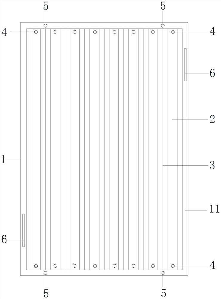
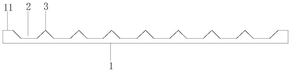
[0031] like Figure 1-Figure 2 As shown, a kind of air guiding plate shown in this embodiment includes a flat plate 1 with a flat surface and a square shape. The upper surface of the plate 1 is provided with several grooves 2 at intervals along its length or width direction. The grooves 2 The cross-section is a trapezoid with a large top and a small bottom, so that the adjacent grooves 2 are separated by an inverted V-shaped support part 3, and at least one air guide hole 4 is provided through the bottom of the groove 2, and the air guide hole can be used for the entire single The grooves are vacuumed, and the upper surface of the flat plate 1 is surrounded by planes 11. After the air guide plate and the production plate are aligned and fixed by using the planar structure, the inner grooves form a sealed structure to realize the air guide holes. Vacuuming operation; in the above, the trapezoidal groove and the inverted V-shaped support part of the air guide plate can prevent t...
Embodiment 2
[0037] A method for making a circuit board shown in this embodiment, which includes a method for improving the poor ink plug hole of the VIA hole of the circuit board window, adopts the air guide plate as described in Example 1 to carry out ink plug hole production, wherein the production board The edge of the plate corresponds to the edge of the air guide plate, and the graphic area of the production plate corresponds to the groove area on the air guide plate. The specific process is as follows:
[0038] (1) Cutting: cut out the core board according to the panel size 520mm×620mm, the thickness of the core board is 0.5mm, and the thickness of the outer layer of copper foil is 0.5oz.
[0039](2) Inner layer circuit production (negative film process): Inner layer graphics transfer, use a vertical coating machine to coat a photosensitive film on the core board, the film thickness of the photosensitive film is controlled at 8 μm, and a fully automatic exposure machine is used to ...
PUM
 Abstract
Description
Claims
Application Information