Eureka AIR delivers breakthrough ideas for toughest innovation challenges, trusted by R&D personnel around the world.

Preparation method of semiconductor substrate and semiconductor structure

A semiconductor and substrate technology, applied in the field of semiconductor substrate and semiconductor structure preparation, can solve the problems of difficulty in preparing GeSn materials, increasing the difficulty of high-quality GeSn materials, and difficulty in obtaining high-quality thin films, etc. The effect of reducing leakage and increasing operating speed

Pending Publication Date: 2021-08-27
INST OF MICROELECTRONICS CHINESE ACAD OF SCI +1
View PDF7 Cites 0 Cited by
  • Summary
  • Abstract
  • Description
  • Claims
  • Application Information

AI Technical Summary

Problems solved by technology

[0003] GeSn will convert from an indirect bandgap material to a direct bandgap material when the Sn composition is about 6%. It is a very promising optoelectronic material among IV compound materials. At the same time, GeSn material has superior carrier mobility than Ge It is an ideal channel material for microelectronic devices. The advantages of the above-mentioned GeSn materials make it the most promising material for Si optoelectronic integration. However, GeSn usually needs to be grown on the Ge buffer layer, and its huge lattice difference causes GeSn As the composition increases, a very large compressive strain will be introduced. This compressive strain requires a higher Sn composition for the transformation of the GeSn material to a direct band gap. However, it is difficult to prepare GeSn materials with a high Sn composition, and it is difficult to obtain high-quality thin films. , increasing the difficulty of growing high-quality GeSn materials

Method used


Image

  • Preparation method of semiconductor substrate and semiconductor structure
  • Preparation method of semiconductor substrate and semiconductor structure
  • Preparation method of semiconductor substrate and semiconductor structure

Examples


Embodiment Construction

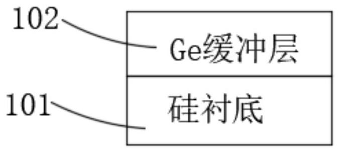
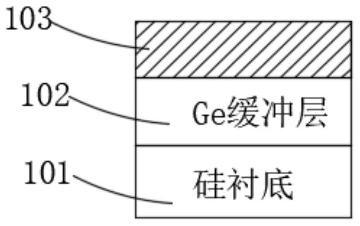
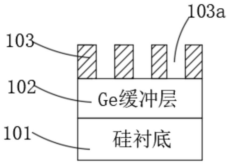
[0024] Hereinafter, embodiments of the present disclosure will be described with reference to the drawings. It should be understood, however, that these descriptions are exemplary only, and are not intended to limit the scope of the present disclosure. Also, in the following description, descriptions of well-known structures and techniques are omitted to avoid unnecessarily obscuring the concept of the present disclosure.

[0025] Various structural schematic diagrams according to embodiments of the present disclosure are shown in the accompanying drawings. The figures are not drawn to scale, with certain details exaggerated and possibly omitted for clarity of presentation. The shapes of the various regions and layers shown in the figure, as well as their relative sizes and positional relationships are only exemplary, and may deviate due to manufacturing tolerances or technical limitations in practice, and those skilled in the art will Regions / layers with different shapes, s...


PUM


Abstract

The invention relates to a preparation method of a semiconductor substrate and a semiconductor structure. The preparation method of the semiconductor structure comprises the following steps: epitaxially growing a germanium buffer layer on a silicon substrate, and growing a first insulating layer on the surface of the germanium buffer layer; performing graphical etching on the first insulating layer to form a plurality of grooves; epitaxially growing a germanium tin layer; providing a supporting substrate, and growing a second insulating layer on the supporting substrate; bonding the supporting substrate with the semiconductor substrate, wherein the second insulating layer is adjacent to the germanium tin layer; and removing the silicon substrate, the germanium buffer layer and the first insulating layer. According to the invention, the germanium tin layer with high quality and high component strain release can be grown.

Description

technical field [0001] The invention relates to the field of semiconductor production technology, in particular to a method for preparing a semiconductor substrate and a semiconductor structure. Background technique [0002] Since the solid solubility of Sn materials in Ge is only 1%, the growth of high-quality and high-composition GeSn materials has been a problem that has plagued the industry for many years. [0003] GeSn will convert from an indirect bandgap material to a direct bandgap material when the Sn composition is about 6%. It is a very promising optoelectronic material among IV compound materials. At the same time, GeSn material has superior carrier mobility than Ge It is an ideal channel material for microelectronic devices. The advantages of the above-mentioned GeSn materials make it the most promising material for Si optoelectronic integration. However, GeSn usually needs to be grown on the Ge buffer layer, and its huge lattice difference causes GeSn As the c...

Claims


Application Information

Patent Timeline
Patent Type & Authority Applications(China)
IPC IPC(8): H01L21/02H01L21/762
CPCH01L21/02381H01L21/0245H01L21/02488H01L21/02502H01L21/02535H01L21/76256
Inventor 亨利·H·阿达姆松孔真真王桂磊
Owner INST OF MICROELECTRONICS CHINESE ACAD OF SCI
Why Eureka
Eureka Blog
Learn More