Occlusion degassing type circuit packaging method

A circuit packaging and degassing technology, applied in the manufacturing of circuits, electrical components, semiconductor/solid-state devices, etc., can solve problems such as hidden dangers of electrical safety, moisture resistance, reduced electrical insulation performance, and integrated circuit manufacturing failures, and reduce porosity. Defects, the effect of improving strength and electrical insulation, improving packing density and flowability

Active Publication Date: 2021-08-27
深圳市耀展科技有限公司
View PDF8 Cites 2 Cited by
  • Summary
  • Abstract
  • Description
  • Claims
  • Application Information

AI Technical Summary

Problems solved by technology

[0005] However, the existing injection molding process is prone to porosity defects. The generation of air bubbles not only reduces the strength of the plastic package, but also greatly reduces the moisture resistance and electrical insulation performance, which will have a great impact on the reliability of the safe use of integrated circuits. Leading to the failure of integrated circuit manufacturing, leaving a safety hazard for the use of electrical appliances

Method used


Image

  • Occlusion degassing type circuit packaging method
  • Occlusion degassing type circuit packaging method
  • Occlusion degassing type circuit packaging method

Examples


Embodiment 1

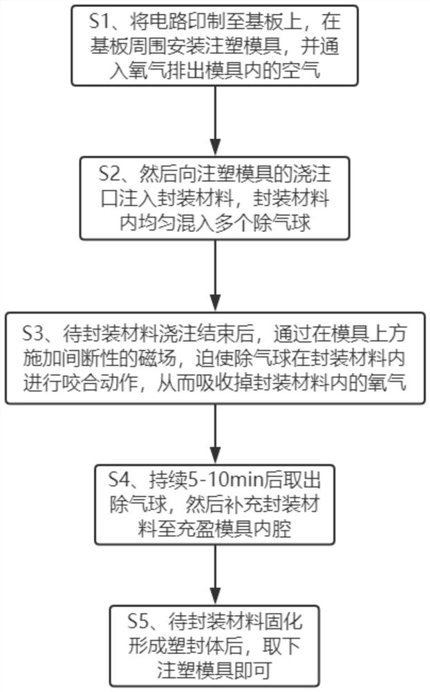
[0046] See Figure 1-2 A biting and devilular circuit packaging method, including the following steps:

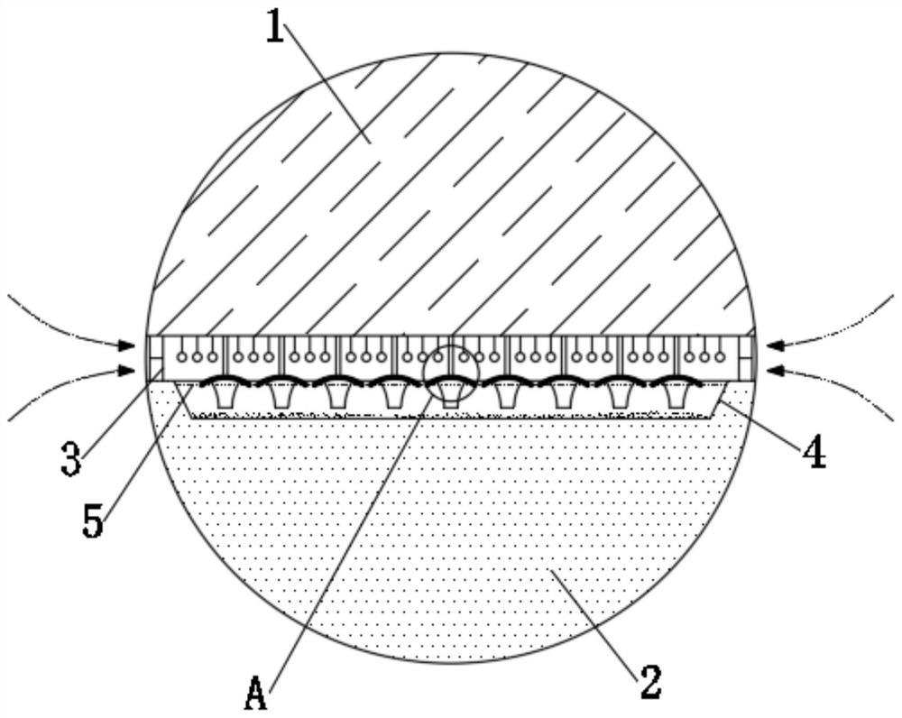
[0047] S1, print the circuit to the substrate, mount the injection mold around the substrate, and enter the air in the oxygen discharge mold;

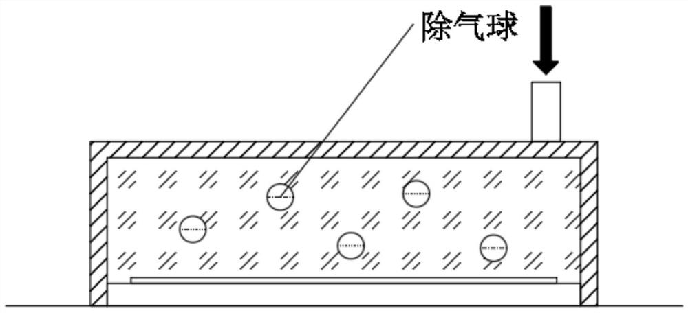
[0048] S2, then inject the packaging material into the casting of the injection mold, evenly mixing the ball in the package material;

[0049] S3, after the pouring of the package material is completed, by applying an intermittent magnetic field above the mold, the balloon is forced to perform a bite operation in the package material, thereby absorbing the oxygen in the package material;

[0050] S4, after 5-10min, remove the balloon, then supplement the packaging material to the inner cavity of the filling mold;

[0051] S5, after the material to be encapsulated materials, after forming a plastic seal, remove the injection mold.

[0052] The substrate uses an alumina substrate, a glass fiber enhanced epoxy resin plate or a glass substra...


PUM


Abstract

The invention discloses an occlusion degassing type circuit packaging method, which belongs to the technical field of circuit packaging, and can exhaust air in an injection mold by introducing oxygen in advance to ensure that gas in a packaging material is basically oxygen, then the oxygen is uniformly mixed into a degassing ball, and an intermittent magnetic field is utilized to trigger the occlusion action of the degassing ball, a large amount of packaging materials can be inhaled when the balloon is opened, then occlusion is carried out under the action of gravity, so that the packaging materials are extruded, oxygen contained in the packaging materials is forced to be released and absorbed, then the packaging materials are discharged out of the balloon, and the occlusion action is repeated, so that the oxygen contained in the packaging materials can be effectively absorbed; and meanwhile, the filling compactness and the fluidity of the packaging material can be improved, the air hole defect easily occurring in the circuit packaging process is greatly reduced, and the strength and the electrical insulating property of a plastic package body are improved.

Description

Technical field [0001] The present invention relates to the field of circuit packaging, and more particularly, to a bite and devilion circuit packaging method. Background technique [0002] The package of the integrated circuit is wrapped on the board to avoid a process technology for the chip to contact outside to prevent external damage to the chip. Impurities and adverse gases in the air, and even water vapor will corrode the precision circuit on the chip, which in turn causes electrical performance to decrease. [0003] After the encapsulation of the integrated circuit, a new package structure-direct bonding type has been developed, and the trial has reached the value of commercialization and has achieved greater development. Direct bonded packages can be quickly developed, and the most important factor is that it can be applied to multi-lead, small spacing, low-cost large-scale automation or semi-active production, and simplifies packaging structure and assembly process. [...

Claims


Application Information

Patent Timeline
Patent Type & Authority Applications(China)
IPC IPC(8): H01L21/56B29C45/34
CPCH01L21/56H01L21/561H01L21/565B29C45/34
Inventor 刘杰夫
Owner 深圳市耀展科技有限公司
Why Eureka
Try Eureka