High-temperature grid bias test method of SiC MOSFET device, computer equipment and storage medium

A technology of high-temperature gate bias and test method, which is applied in the direction of single semiconductor device test, instrument, measurement device, etc., and can solve problems such as not considering the dependence of threshold voltage time

Active Publication Date: 2021-09-07
CHINA ELECTRONICS PROD RELIABILITY & ENVIRONMENTAL TESTING RES INST
View PDF6 Cites 5 Cited by
  • Summary
  • Abstract
  • Description
  • Claims
  • Application Information

AI Technical Summary

Problems solved by technology

[0003] Based on this, it is necessary to provide a high temperature gate bias test method for SiC MOSFET devices, computer equipment and storage devices for the existing high temperature gate bias test method, which does not consider the dependence of threshold voltage on gate bias voltage change on time. medium

Method used


Image

  • High-temperature grid bias test method of SiC MOSFET device, computer equipment and storage medium
  • High-temperature grid bias test method of SiC MOSFET device, computer equipment and storage medium
  • High-temperature grid bias test method of SiC MOSFET device, computer equipment and storage medium

Examples


Embodiment Construction

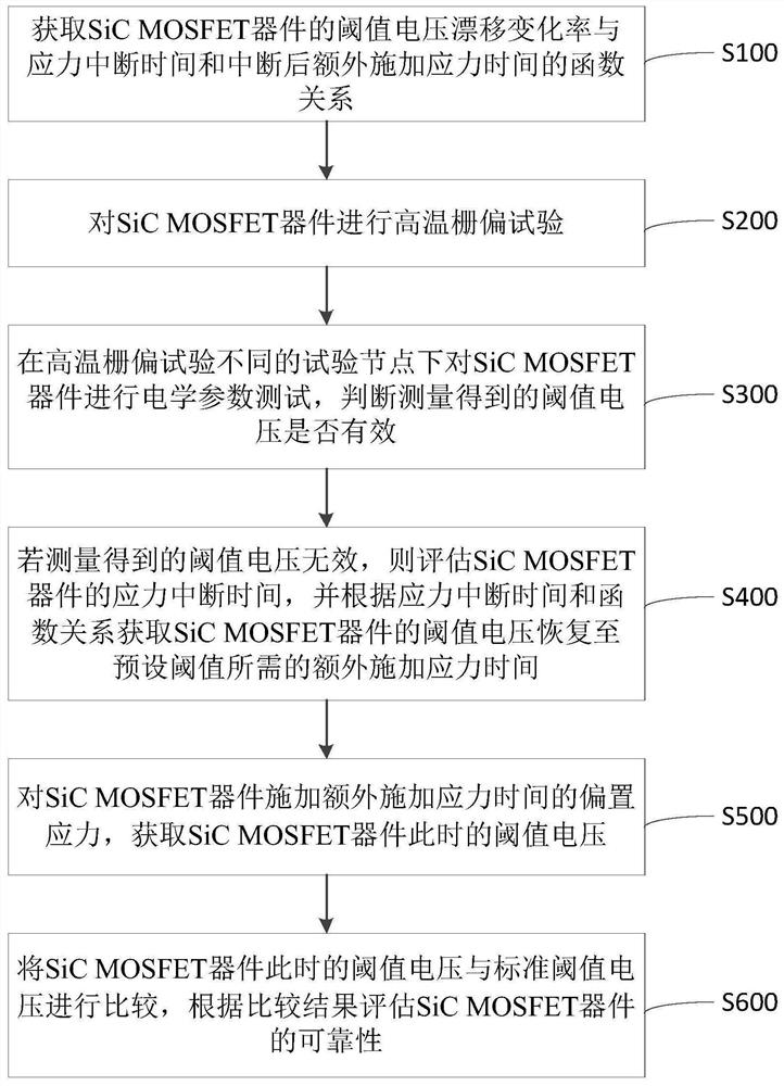
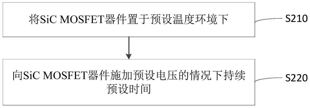
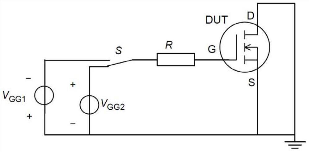
[0023] In order to facilitate understanding of the present invention, the present invention will be described more fully described with reference to the related drawings. A preferred embodiment of the present invention is given in the drawings. However, the present invention can be implemented in many different forms, is not limited to the embodiments described herein. Conversely, the purpose of providing these embodiments is to be more thoroughly comprehensively understood to understand the disclosure of the present invention.

[0024] It should be noted that when the element is referred to as "fixed to" another element, it can be directly in another element or may also exist. When a component is considered to be "connected" another element, it may be directly connected to another element or may always exist in the center element. The term "vertical", "horizontal", "left", "right", as used herein, "upper", "lower", "front", "rear", "circumferential" and similar expressions are ba...


PUM


Abstract

The invention relates to the technical field of high-temperature grid bias tests, and discloses a high-temperature grid bias test method of a SiC MOSFET device, a computer device and a storage medium. When electrical parameter tests are carried out on the SiC MOSFET device in different test nodes for carrying out the high-temperature grid bias test on the SiC MOSFET device, if the measurement of the SiC MOSFET device is not completed in time, stress interruption time of the SiC MOSFET device can be evaluated, extra stress application time of the SiC MOSFET device can be obtained according to a pre-obtained function relation between a threshold voltage drift change rate of the SiC MOSFET device and the stress interruption time and the extra stress application time after interruption, the bias stress of the extra stress application time is applied to the SiC MOSFET device, so that after a threshold voltage on the SiC MOSFET device is recovered to a preset threshold value, and the SiC MOSFET device is measured in time, thereby guaranteeing that the measured threshold voltage can represent the real drift condition of the SiC MOSFET device at the moment.

Description

Technical field [0001] The present invention relates to a high temperature gate bias test technology, and particularly relates to one kind of high temperature SiC MOSFET device gate bias test methods, apparatus and computer storage media. Background technique [0002] SiC as a typical third generation of semiconductor material having a large band gap, high critical breakdown field, high electron saturation velocity and high thermal conductivity, etc., are very suitable for producing high temperature, high pressure power electronic devices, and radiation of power. In the SiC (silicon carbide) power device family, SiC MOSFET device (silicon carbide metal-oxide semiconductor field effect transistor) having a high working frequency, low switching losses, low on-resistance and high current density, etc., can significantly improve power system the switching frequency and the overall efficiency. Currently, SiC MOSFET device comprises a major reliability issue, the threshold voltage stab...

Claims


Application Information

Patent Timeline
Patent Type & Authority Applications(China)
IPC IPC(8): G01R31/26
CPCG01R31/2601
Inventor 陈媛来萍张鹏贺致远陈义强刘昌徐新兵
Owner CHINA ELECTRONICS PROD RELIABILITY & ENVIRONMENTAL TESTING RES INST
Why Eureka
Try Eureka