Supercharge Your Innovation With Domain-Expert AI Agents!

Semiconductor cleaning equipment

A technology for cleaning equipment and semiconductors, which is applied in semiconductor/solid-state device manufacturing, cleaning methods using liquids, cleaning methods, and utensils. It can solve problems affecting cleaning efficiency and cleaning balance, reduce acoustic energy, etc., and improve energy utilization. The effect of improving the cleaning efficiency

Pending Publication Date: 2021-09-07
BEIJING NAURA MICROELECTRONICS EQUIP CO LTD
View PDF0 Cites 1 Cited by
  • Summary
  • Abstract
  • Description
  • Claims
  • Application Information

AI Technical Summary

Problems solved by technology

like Figure 8 As shown, when sound waves enter the air bubbles from water, there will be refraction and reflection of waves, forming refracted sound waves and emitting sound waves, thereby reducing the sound wave energy entering the cleaning tank 6, affecting cleaning efficiency and cleaning balance

Method used


Image

  • Semiconductor cleaning equipment
  • Semiconductor cleaning equipment
  • Semiconductor cleaning equipment

Examples


Embodiment Construction

[0031] Specific embodiments of the present invention will be described in detail below in conjunction with the accompanying drawings. It should be understood that the specific embodiments described here are only used to illustrate and explain the present invention, and are not intended to limit the present invention.

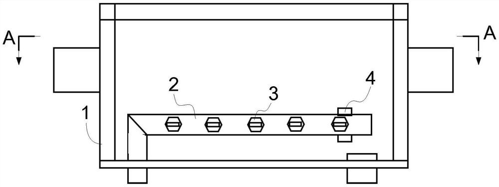
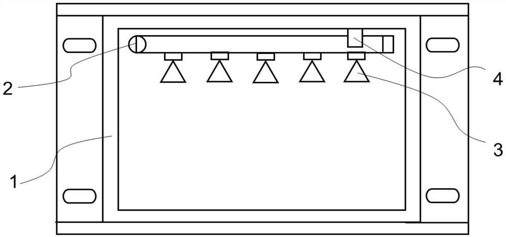
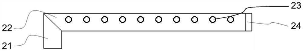
[0032] Such as Figure 9 Shown is a cleaning equipment structure in the prior art to improve the utilization rate of transducer acoustic energy, wherein the bottom plate of the cleaning tank 6 is designed to form a certain angle σ with the horizontal plane. At this time, the air bubbles 7 attached to the bottom plate of the cleaning tank 6 The stress situation is as Figure 10 As shown, it is subject to its own gravity G, the buoyancy F exerted by the conductive medium 8, and the positive pressure F exerted by the bottom plate of the cleaning tank 6 N And the downward friction force f of the parallel bottom plate. Since the gravity G of the bubble itself is mu...


PUM


Abstract

The invention provides semiconductor cleaning equipment which comprises a bath, a cleaning tank, a sound wave signal generating device and a conducting medium spraying device. The cleaning tank is used for containing a wafer, and the bottom of the cleaning tank is contained in the bath. The sound wave signal generating device is arranged at the bottom of the bath and used for providing sound wave signals. A conducting medium in the bath is used for conducting the sound wave signals to the cleaning tank. The conducting medium spraying device is arranged in the bath and located on one side of the cleaning tank and is used for spraying the conducting medium to the bottom of the cleaning tank so as to form a conducting medium layer flowing in a directional mode at the bottom of the cleaning tank. According to the invention, the conducting medium spraying device is arranged in the bath and can spray the conducting medium to the bottom of the wafer cleaning tank to form a conducting medium layer continuously flowing from one side of the cleaning tank to the other side of the cleaning tank at the bottom of the wafer cleaning tank, and bubbles at the bottom of the wafer cleaning tank are pushed away from the bottom of the wafer cleaning tank, so that the energy utilization rate of the sound wave signals is improved, and the wafer cleaning efficiency is improved.

Description

technical field [0001] The present invention relates to the field of semiconductor process equipment, in particular to semiconductor cleaning equipment. Background technique [0002] Silicon wafer surface cleaning is an important link in the wafer production process. In the prior art, the wafer is usually cleaned by megasonic cleaning technology. The specific principle is to apply high-frequency megasonic waves to the cleaning solution of the wafer, so that the molecules of the cleaning solution Accelerated movement under the action produces high-speed fluid waves and continuously impacts the surface of the wafer to forcibly remove the pollutants and fine particles adsorbed on the surface of the wafer, thereby achieving high-efficiency and high-quality cleaning effects. [0003] Such as Figure 10 Shown is a schematic diagram of the principle of megasonic components used in semiconductor cleaning equipment at this stage. The transducer 5 placed under the cleaning tank 6 tran...

Claims


Application Information

Patent Timeline
Patent Type & Authority Applications(China)
IPC IPC(8): H01L21/67B08B3/12B08B3/02
CPCH01L21/67057B08B3/12B08B3/02
Inventor 张亚斌赵宏宇姬庆韬
Owner BEIJING NAURA MICROELECTRONICS EQUIP CO LTD
Features
  • R&D
  • Intellectual Property
  • Life Sciences
  • Materials
  • Tech Scout
  • Unparalleled Data Quality
  • Higher Quality Content
  • 60% Fewer Hallucinations
Learn More