Two-dimensional negative quantum capacitance transistor device and preparation method thereof

A negative quantum and transistor technology, applied in semiconductor/solid-state device manufacturing, semiconductor devices, electrical components, etc., can solve the problems of unsatisfactory device switching speed, hysteresis behavior, and slow ferroelectric flipping rate.

Active Publication Date: 2021-09-07
FUDAN UNIV
View PDF3 Cites 0 Cited by
  • Summary
  • Abstract
  • Description
  • Claims
  • Application Information

AI Technical Summary

Problems solved by technology

[0004] The traditional negative capacitance effect occurs during the polarization reversal of ferroelectric materials. However, the ferroelectric revers

Method used


Image

  • Two-dimensional negative quantum capacitance transistor device and preparation method thereof
  • Two-dimensional negative quantum capacitance transistor device and preparation method thereof
  • Two-dimensional negative quantum capacitance transistor device and preparation method thereof

Examples


Embodiment Construction

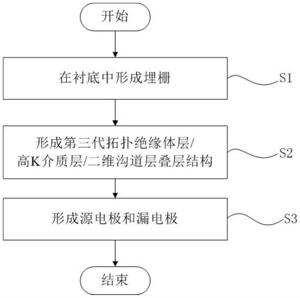
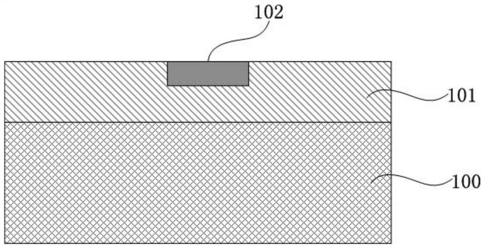
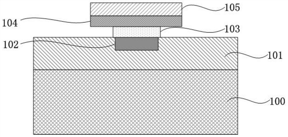
[0017] In order to make the purpose, technical solutions and advantages of the present invention clearer, the technical solutions in the embodiments of the present invention will be clearly and completely described below in conjunction with the accompanying drawings in the embodiments of the present invention. It should be understood that the specific The examples are only used to explain the present invention, not to limit the present invention. The described embodiments are only some, not all, embodiments of the present invention. Based on the embodiments of the present invention, all other embodiments obtained by persons of ordinary skill in the art without making creative efforts belong to the protection scope of the present invention.

[0018] In the description of the present invention, it should be noted that the orientation or positional relationship indicated by the terms "upper", "lower", "vertical" and "horizontal" are based on the orientation or positional relation...


PUM


Abstract

The invention discloses a two-dimensional negative quantum capacitance transistor device and a preparation method thereof. The two-dimensional negative quantum capacitance transistor device comprises a substrate; a buried gate which is formed in the substrate, wherein the upper surface of the buried gate is flush with the upper surface of the substrate; a third-generation topological insulator layer which is formed on the buried gate, wherein the length of the third-generation topological insulator layer is equal to that of the buried gate; a high-K dielectric layer which covers the third-generation topological insulator layer; a two-dimensional channel layer which is formed on the high-K dielectric layer, wherein the two-dimensional channel layer and the third-generation topological insulator layer have a common area; a source electrode and a drain electrode which are formed on the substrate and the two sides of the two-dimensional channel layer respectively, partially cover the two-dimensional channel layer and are not overlapped with the buried gate, wherein the topological insulator layer provides negative quantum capacitance, so the total capacitance of the gate is increased, and the sub-threshold swing is reduced.

Description

technical field [0001] The invention relates to the technical field of semiconductor manufacturing, in particular to a two-dimensional negative quantum capacitance transistor device and a preparation method thereof. Background technique [0002] With the further scaling down of the feature size of semiconductor devices, the ever-increasing power consumption in complementary metal-oxide-semiconductor (CMOS) circuits has become an urgent problem to be solved. [0003] As the device size decreases, the operating voltage needs to be reduced to reduce power consumption. However, the reduction of the operating voltage is limited by the Boltzmann limit. In order to solve this problem, some novel devices with subthreshold swing (SS) below 60mV / dec at room temperature have been proposed, such as the negative capacitance field effect Transistor (NCFET) for low-power operation through an internal voltage amplification mechanism. [0004] The traditional negative capacitance effect oc...

Claims


Application Information

Patent Timeline
IPC IPC(8): H01L29/423H01L29/78H01L21/34H01L21/44
CPCH01L29/78H01L29/66969H01L29/401H01L29/42356H01L29/42364
Inventor 朱颢张凯杨雅芬孙清清
Owner FUDAN UNIV
Why Eureka
Try Eureka