
Method for improving performance of image sensor

An image sensor and performance technology, used in image communication, color TV components, TV system components, etc., can solve problems such as limited, large chip area, power consumption cost, and unfavorable overall performance of image sensors.

Pending Publication Date: 2021-09-10
GALAXYCORE SHANGHAI
View PDF17 Cites 0 Cited by
  • Summary
  • Abstract
  • Description
  • Claims
  • Application Information

AI Technical Summary

Problems solved by technology

[0004] One is to group the column-parallel ADC arrays so that the inversions will not be concentrated at the same time, but relatively scattered at multiple times, weakening the impact of simultaneous inversions, but this method is useful for reducing the inversions caused by simultaneous inversions. Noise crosstalk, the effect of improving image sensor performance is relatively limited;
[0005] The other is to strengthen the lateral drive and use a stronger lateral signal to minimize the crosstalk caused by concentrated flipping through the lateral signal. However, this method requires a stronger lateral drive, which requires additional introduction of a larger chip area, Power consumption and cost are not conducive to the improvement of the overall performance of the image sensor

Method used


Image

  • Method for improving performance of image sensor
  • Method for improving performance of image sensor
  • Method for improving performance of image sensor

Examples


Embodiment 1

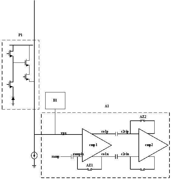
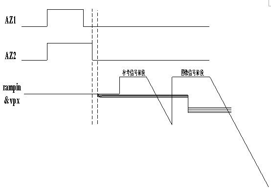
[0035] figure 1 , figure 2 A method for improving the performance of an image sensor according to Embodiment 1 of the present invention is shown.

[0036] exist figure 1 In the image sensor circuit shown, the region P1 is a pixel array, and the region A1 is a column-parallel ADC. Since the comparator cmp1 in the column-parallel ADC circuit (here, the first-stage comparator in the two-stage comparator is taken as an example, this paper Those skilled in the art can understand that in other preferred embodiments not shown, the offset signal can also be introduced by any one of the other numbers of multi-level comparators) The self-clearing technology is adopted, so that the DC blocking capacitor During self-clearing, the offset signal related to the pixel level is completely cut off, so the offset signal related to the pixel level needs to be introduced through the clamping circuit module B1.

[0037] Specifically, the output signal vpx of the pixel array P1 is clamped by the...

Embodiment 2

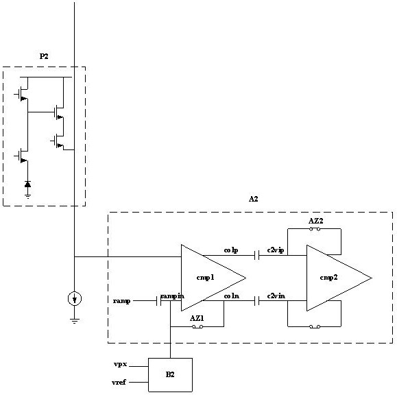
[0039] Figure 3-Figure 5 A method for improving the performance of an image sensor according to Embodiment 2 of the present invention is shown.

[0040] exist image 3 In the image sensor circuit shown, the region P2 is a pixel array, and the region A2 is a column-parallel ADC. Since the comparator cmp1 in the column-parallel ADC circuit (the first-stage comparator in the two-stage comparator is taken as an example here, this Those skilled in the art can understand that in other preferred embodiments not shown, the offset signal can also be introduced by any one of the other numbers of multi-level comparators) The self-clearing technology is adopted, so that the DC blocking capacitor During self-clearing, the offset signal related to the pixel level is completely cut off, so the offset signal related to the pixel level needs to be introduced through the random charge injection module B2.

[0041] Specifically, after the self-clearing is completed, a signal of random size is...

Embodiment 3

[0043] Figure 6-Figure 9 A method for improving the performance of an image sensor according to Embodiment 3 of the present invention is shown.

[0044] exist Figure 6 In the image sensor circuit shown, the region P3 is a pixel array, and the region A3 is a column-parallel ADC, and its circuit structure is similar to that of the prior art, without introducing additional circuit modules. The structure of the first-stage comparator cmp1 is as follows Figure 7 shown.

[0045] Such as Figure 8 As shown, since the DC blocking capacitor at the pixel input terminal of the first-stage comparator is removed, when the first-stage comparator is self-clearing, the first-stage comparator samples the offset signal at the pixel level. After the self-clearing of the switched capacitor AZ1_a is completed, The output of the high and low gain points of the first-stage comparator is switched, and the offset signal is transferred from co1n to co1p. At this time, by sampling the offset sign...


PUM


Abstract

The invention provides a method for improving the performance of an image sensor, and the method comprises the steps: introducing a pixel-level-related offset signal into a reference signal, enabling the reference signals of different columns in the same row to change based on the pixel-level-related offset signal, reducing crosstalk caused by concentrated overturning of the column parallel analog-to-digital converter in the reference signal stage of the image sensor, improving the imaging quality, adopting random signals in a chip directly. In this way, an additional random signal generator is not needed, the area, power consumption and cost of the chip are not greatly influenced, and the overall performance of the image sensor is improved.

Description

technical field [0001] The present invention relates to a method of improving the performance of an image sensor. Background technique [0002] At present, correlated double sampling (CDS) technology is usually used in CMOS image sensors (CIS) to eliminate the low-frequency noise related to the misadjusted signal of the signal path. Generally, the signal path is required to have two analog-to-digital conversions, and one is to perform analog-to-digital conversion when the pixel unit is reset. Quantization to obtain the reference signal value ref, the second time is to release the photogenerated electronic signal of the pixel unit and quantize it to obtain the image signal value sig, so the difference between these two times is the actual signal value. The premise of using the difference between two quantizations to do CDS is that the two quantizations are non-correlated. Compared with the second quantized image signal value sig, the first quantized reference signal value re...

Claims


Application Information

Patent Timeline
IPC IPC(8): H04N5/374
CPCH04N25/76
Inventor 赵立新乔劲轩范爱鹏
Owner GALAXYCORE SHANGHAI
Learn More