Eureka AIR delivers breakthrough ideas for toughest innovation challenges, trusted by R&D personnel around the world.

Deep Schottky power device with buried layer structure and preparation method of deep Schottky power device

A power device and layer structure technology, which is applied in semiconductor/solid-state device manufacturing, semiconductor devices, electrical components, etc., and can solve the problems of large device cell area and large MOSFET device Schottky junction area.

Pending Publication Date: 2021-09-14
GLOBAL POWER TECH CO LTD
View PDF0 Cites 0 Cited by
  • Summary
  • Abstract
  • Description
  • Claims
  • Application Information

AI Technical Summary

Problems solved by technology

[0004] The technical problem to be solved by the present invention is to provide a deep Schottky power device with a buried layer structure and its preparation method, which solves the problem that the MOSFET device Schottky junction area of ​​the traditional integrated junction barrier Schottky diode is too large, resulting in The problem that the cell area of ​​the whole device is too large

Method used


Image

  • Deep Schottky power device with buried layer structure and preparation method of deep Schottky power device
  • Deep Schottky power device with buried layer structure and preparation method of deep Schottky power device
  • Deep Schottky power device with buried layer structure and preparation method of deep Schottky power device

Examples


Embodiment Construction

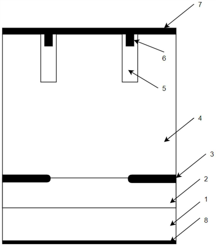
[0041] see figure 1 As shown, the present invention has a deep Schottky power device with a buried layer structure, comprising:

[0042] A substrate layer 1, the substrate layer 1 is an N+ substrate, and the doping concentration is 5×10 18 cm -3 Made of SiC material, thickness 350μm;

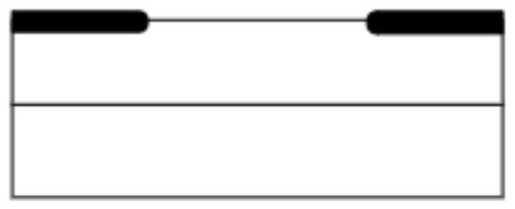
[0043] A buffer layer 2, the buffer layer 2 is arranged on the upper side of the substrate layer 1, the thickness of the buffer layer 2 is 2 μm to 3 μm, and the material is N ion-doped 4H-SiC;

[0044] At least one buried layer 3, the buried layer 3 is arranged on the upper side of the buffer layer 2, the width of the buried layer 3 is smaller than the width of the buffer layer 2, the thickness of the buried layer 3 is 0.1 μm to 0.2 μm, and the length is 1μm~3μm, the material is 4H-SiC doped with P ions;

[0045] A drift layer 4, the drift layer 4 is arranged on the upper side of the buffer layer 2, the buried layer 3 is arranged between the buffer layer 4 and the drift layer 2, and the drif...


PUM

PropertyMeasurementUnit
Thicknessaaaaaaaaaa
Thicknessaaaaaaaaaa
Lengthaaaaaaaaaa

Abstract

The invention provides a deep Schottky power device with a buried layer structure and a preparation method of the deep Schottky power device. The device comprises a substrate layer, a buffer layer, at least one buried layer, a drift layer, at least one insulation type polycrystalline silicon layer,at least one Schottky contact electrode, an anode and a cathode; the buffer layer is arranged on the upper side surface of the substrate layer; the buried layer is arranged on the upper side surface of the buffer layer, and the width of the buried layer is smaller than that of the buffer layer; the drift layer is arranged on the upper side surface of the buffer layer, the buried layer is arranged between the buffer layer and the drift layer, and the drift layer is provided with at least one drift groove; the at least one insulation type polycrystalline silicon layer is arranged in the drift groove, and the insulation type polycrystalline silicon layer is provided with a polycrystalline silicon groove; the Schottky contact electrode is arranged in the polycrystalline silicon groove; the anode is arranged on the drift layer and is connected with the insulation type polycrystalline silicon layer and the Schottky contact electrode; and the cathode is connected to the lower side surface of the substrate layer. The problem that the cellular area of the device is too large is solved.

Description

technical field [0001] The invention relates to a deep Schottky power device with a buried layer structure and a preparation method thereof. Background technique [0002] As a wide bandgap semiconductor device, SiC Schottky barrier diode first replaces Si devices in the field of power electronics technology. SiC Schottky barrier diodes suppress the leakage of devices in the field of power electronics and improve the breakdown voltage of devices. At present, commercialized SiC Schottky barrier diodes have been widely used in various high-frequency switching power supplies, power factor correction, and motor drives. When used in combination with power MOSFETs, the switching frequency can reach 600kHz and is expected to be higher than 1MHz. Some companies use SiC Schottky barrier diodes instead of Si fast recovery diodes in IGBT frequency conversion or inverter devices to increase revenue. [0003] In recent years, with the continuous development of power electronic systems, ...

Claims


Application Information

Patent Timeline
IPC IPC(8): H01L29/78H01L29/06H01L21/336
CPCH01L29/78H01L29/0619H01L29/0684H01L29/66068
Inventor 张瑜洁施广彦刘刚李志君黄波
Owner GLOBAL POWER TECH CO LTD
Why Eureka
Eureka Blog
Learn More