Heterojunction power device and manufacturing method thereof

A power device and heterojunction technology, applied in the field of microelectronics, can solve problems such as poor passivation process repeatability, and achieve the effects of suppressing current collapse effect, improving reverse voltage withstand capability, and increasing forward blocking voltage.

Active Publication Date: 2021-05-07
XIDIAN UNIV
View PDF6 Cites 5 Cited by
  • Summary
  • Abstract
  • Description
  • Claims
  • Application Information

AI Technical Summary

Problems solved by technology

However, the repeatability of the passivation process is poor, and the current collapse can only be suppressed at a relatively low bias voltage. When the device is biased at a high voltage, the current collapse is still very serious

Method used


Image

  • Heterojunction power device and manufacturing method thereof
  • Heterojunction power device and manufacturing method thereof
  • Heterojunction power device and manufacturing method thereof

Examples


Embodiment 1

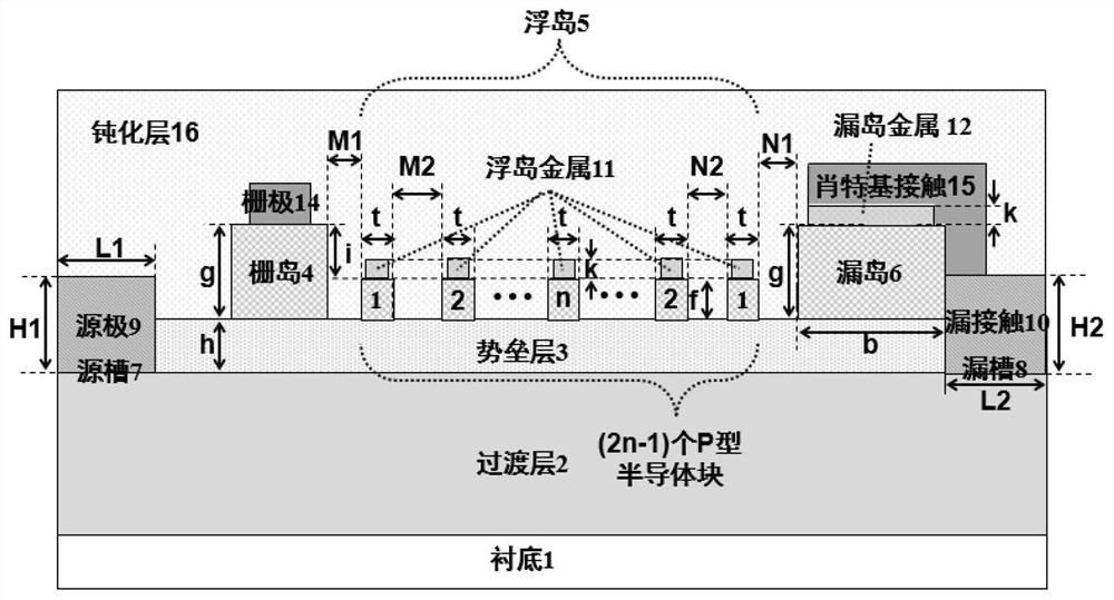
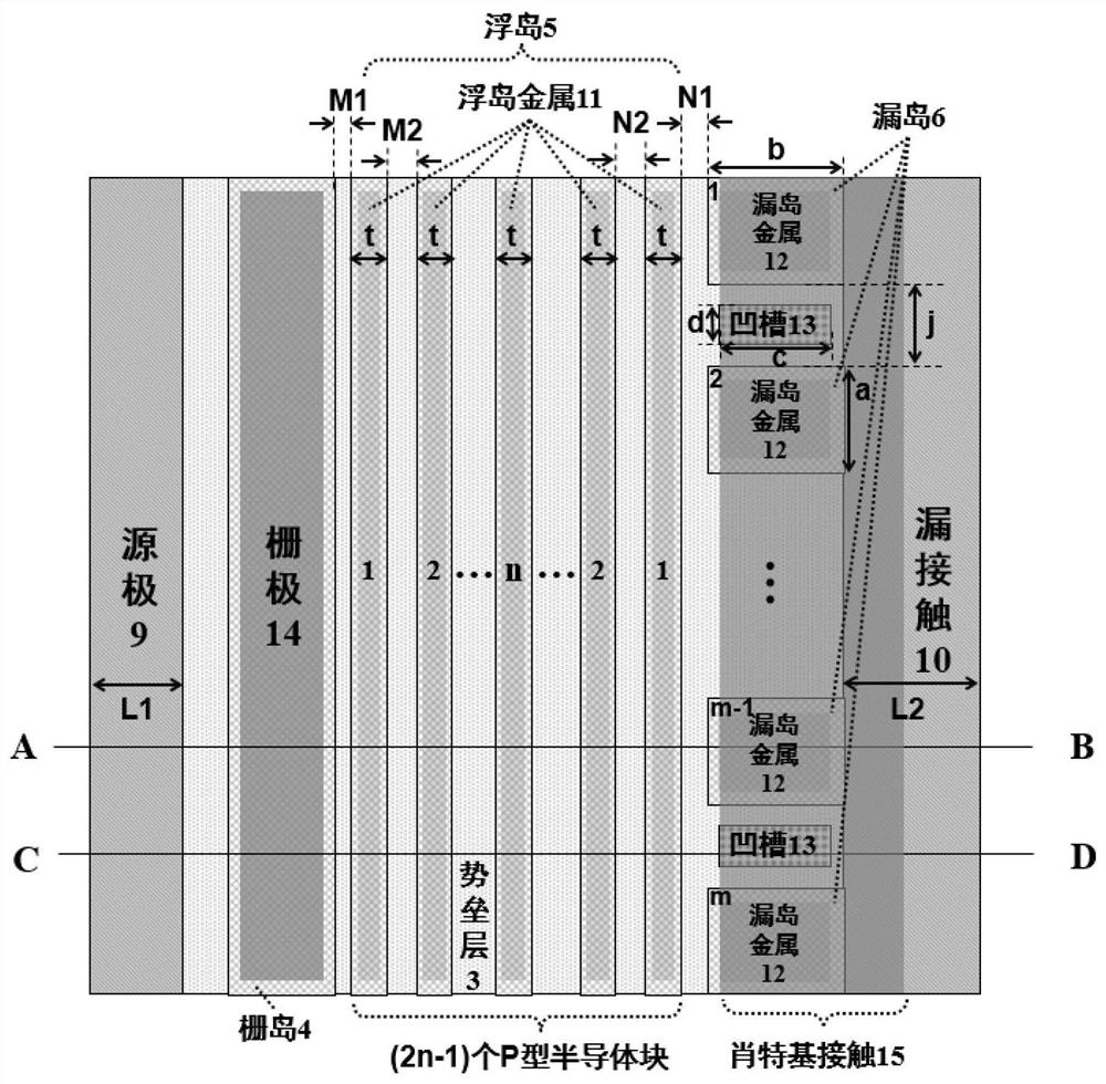
[0061] Embodiment 1: Using a sapphire substrate to fabricate the floating island 5 and the leaky island 6 with a height f of 1 nm and a doping concentration of 4×10 15 cm -3 , the number of independent P-type semiconductor blocks in the floating island 5 is one, the number of semiconductor cuboid blocks in the drain island 6 is two, and the number of grooves is one heterojunction power device.

[0062]Step 1. Epitaxial GaN material is made transition layer 2 on sapphire substrate 1, as Figure 5 a.

[0063] 1a) GaN material with a thickness of 30nm is epitaxially grown on the sapphire substrate 1 by metal-organic chemical vapor deposition technology. The source flow rate is 20μmol / min;

[0064] 1b) GaN material with a thickness of 0.97 μm is epitaxially grown on the GaN material by metal-organic chemical vapor deposition technology to form an undoped transition layer 2. The process conditions are as follows: temperature is 960° C., pressure is 45 Torr, and hydrogen flow rat...

Embodiment 2

[0092] Embodiment 2: The height f of the floating island 5 and the leaky island 6 is 200 nm, and the doping concentration is 5×10 using a silicon carbide substrate. 17 cm -3 , the number of independent P-type semiconductor blocks in the floating island 5 is five, the number of semiconductor cuboid blocks in the drain island 6 is three, and the number of grooves is two heterojunction power devices.

[0093] Step 1. Epitaxially AlN and GaN materials on the silicon carbide substrate 1 to form the transition layer 2, such as Figure 5 a.

[0094] 1.1) Metal-organic chemical vapor deposition technology is used at a temperature of 1000° C., a pressure of 45 Torr, a flow rate of hydrogen gas of 4600 sccm, a flow rate of ammonia gas of 4600 sccm, and a flow rate of aluminum source of 5 μmol / min, on the silicon carbide substrate 1 Undoped AlN material with an epitaxial thickness of 100nm;

[0095] 1.2) Using metal-organic chemical vapor deposition technology, the epitaxial thickness...

Embodiment 3

[0118] Embodiment 3: Using a silicon substrate to make the floating island 5 and the leaky island 6, the height f is 400nm, and the doping concentration is 5×10 20 cm -3 A heterojunction power device in which the number of independent P-type semiconductor blocks in the floating island 5 is 7, the number of semiconductor cuboid blocks in the drain island 6 is 7, and the number of grooves is 6.

[0119] Step A. Epitaxial AlN and GaN materials on the silicon substrate 1 from bottom to top to make the transition layer 2, such as Figure 5 a.

[0120] A1) AlN material with a thickness of 400nm is epitaxially grown on the silicon substrate 1 by metal-organic chemical vapor deposition technology. The source flow rate is 25μmol / min;

[0121] A2) Use metal organic chemical vapor deposition technology to epitaxially GaN material with a thickness of 8.6 μm on AlN material to complete the fabrication of transition layer 2. The flow rate is 4000 sccm, and the gallium source flow rate i...


PUM

PropertyMeasurementUnit
heightaaaaaaaaaa
heightaaaaaaaaaa
lengthaaaaaaaaaa

Abstract

The invention discloses a heterojunction power device and a manufacturing method thereof, and mainly solves the problems of current collapse phenomenon and low breakdown voltage of the existing gallium nitride-based device. The heterojunction power device comprises a substrate (1), a transition layer (2), a barrier layer (3), a source groove (7), a drain groove (8), a source electrode (9), a drain contact (10), floating island metal (11), drain island metal (12), a grid electrode (14) and a passivation layer (16), wherein a gate island (4), a floating island (5) and a drain island (6) are sequentially arranged on the barrier layer from left to right; the floating island (5) is composed of 2n-1 independent P-type semiconductor blocks, the drain island (6) is composed of m P-type semiconductor cuboid blocks, and a groove (13) is formed between every two cuboid blocks; and metal is deposited on the inner portion, the front side, the rear side and the right side of the groove to form Schottky contact (15). Current collapse can be restrained, breakdown voltage is improved, forward blocking and reverse blocking are good, and the heterojunction power device can be used for a basic device of a power electronic system.

Description

technical field [0001] The invention belongs to the technical field of microelectronics, and particularly relates to a heterojunction power device, which can be used as a basic device of a power electronic system. [0002] technical background [0003] Power electronic systems are widely used in many fields such as aerospace, industrial equipment, electric vehicles, and household appliances. Power devices, as important components of power electronic systems, are important tools for energy conversion and control. Therefore, the performance and reliability of power devices have a decisive impact on the technical indicators and performance of the entire power electronic system. [0004] At present, the performance of Si-based and GaAs-based semiconductor power devices has approached their theoretical limits. In order to break through the current research and development bottleneck of semiconductor power devices and further improve the performance of power systems, heterojunctio...

Claims


Application Information

Patent Timeline
Patent Type & Authority Applications(China)
IPC IPC(8): H01L29/06H01L29/20H01L29/417H01L29/423H01L29/778H01L21/335
CPCH01L29/0611H01L29/2003H01L29/41725H01L29/42316H01L29/778H01L29/66462
Inventor 毛维刘晓雨杨翠杜鸣高北鸾王海永马佩军赵胜雷张进成郝跃
Owner XIDIAN UNIV
Why Eureka
Try Eureka