

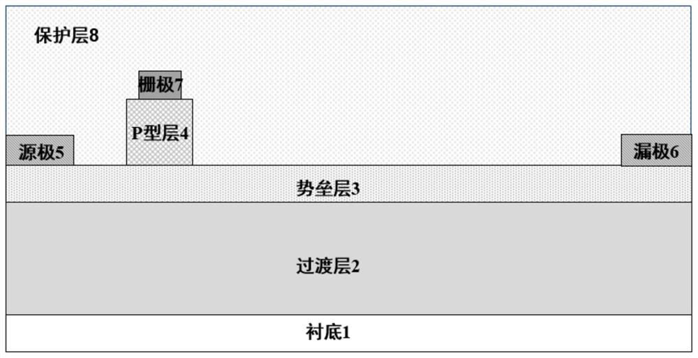
GaN-based high-electron-mobility transistor and manufacturing method thereof
A high electron mobility, gallium nitride-based technology, applied in the field of gallium nitride-based high electron mobility transistors, can solve problems such as poor passivation process repeatability
- Summary
- Abstract
- Description
- Claims
- Application Information
AI Technical Summary
Problems solved by technology
Method used
Image

Examples
Embodiment 1
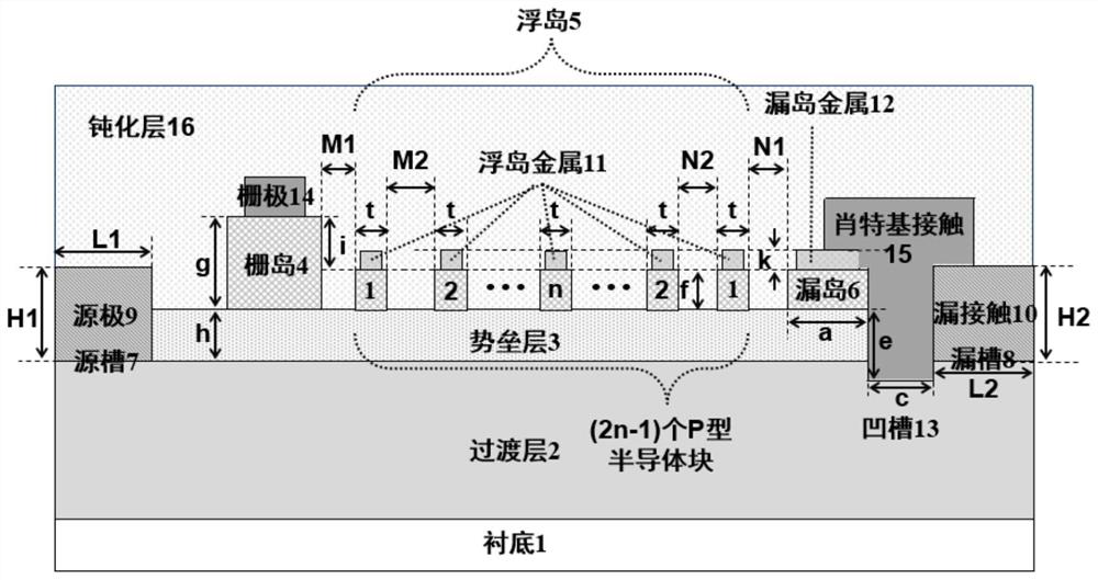
[0059] Embodiment 1: Using a sapphire substrate to fabricate the floating island 5 and the leaky island 6 with a height f of 1 nm and a doping concentration of 4×10 15 cm -3 , the number of independent P-type semiconductor blocks in the floating island 5 is one, and the number of semiconductor cuboid blocks in the drain island 6 is one gallium nitride-based high electron mobility transistor.
[0060] Step 1. Epitaxial GaN material is made transition layer 2 on sapphire substrate 1, as Figure 4 a.
[0061] 1a) GaN material with a thickness of 30nm was epitaxially grown on the sapphire substrate 1 by metal-organic chemical vapor deposition technology. The source flow rate is 22μmol / min;
[0062]1b) GaN material with a thickness of 0.97 μm is epitaxially grown on the GaN material by metal-organic chemical vapor deposition technology to form an undoped transition layer 2. The process conditions are as follows: temperature is 960° C., pressure is 45 Torr, and hydrogen flow rate...
Embodiment 2
[0090] Embodiment 2: The height f of the floating island 5 and the leaky island 6 is 200 nm, and the doping concentration is 5×10 using a silicon carbide substrate. 17 cm -3 , the number of independent P-type semiconductor blocks in the floating island 5 is five, and the number of semiconductor cuboid blocks in the drain island 6 is three GaN-based high electron mobility transistors.
[0091] Step 1. Epitaxially AlN and GaN materials on the silicon carbide substrate 1 to form the transition layer 2, such as Figure 4 a.
[0092] 1.1) Metal-organic chemical vapor deposition technology is used at a temperature of 1000° C., a pressure of 45 Torr, a hydrogen flow rate of 4600 sccm, an ammonia gas flow rate of 4600 sccm, and an aluminum source flow rate of 5 μmol / min, on a silicon carbide substrate 1 Undoped AlN material with an epitaxial thickness of 100nm;
[0093] 1.2) Using metal-organic chemical vapor deposition technology, the epitaxial thickness on the AlN material is Th...
Embodiment 3
[0116] Embodiment 3: Using a silicon substrate to make the floating island 5 and the leaky island 6, the height f is 400nm, and the doping concentration is 5×10 20 cm -3 , the number of independent P-type semiconductor blocks in the floating island 5 is seven, and the number of semiconductor cuboid blocks in the drain island 6 is seven GaN-based high electron mobility transistors.
[0117] Step A. Epitaxial AlN and GaN materials on the silicon substrate 1 from bottom to top to make the transition layer 2, such as Figure 4 a.
[0118] First, AlN material with a thickness of 400nm is epitaxially grown on silicon substrate 1 by metal-organic chemical vapor deposition technology. The source flow rate is 25μmol / min;
[0119] Then, GaN material with a thickness of 8.6 μm was epitaxially grown on the AlN material by metal-organic chemical vapor deposition technology to complete the fabrication of the transition layer 2. The flow rate is 4000 sccm, and the gallium source flow rat...
PUM
| Property | Measurement | Unit |
|---|---|---|
| height | aaaaa | aaaaa |
| height | aaaaa | aaaaa |
| width | aaaaa | aaaaa |
Abstract
Description
Claims
Application Information