III-nitride enhanced-mode metal-insulator-semiconductor high electron mobility transistor (MISHEMT) device

An enhanced, nitride technology, applied in the direction of semiconductor devices, electrical components, circuits, etc., can solve problems such as unsatisfactory effects

Inactive Publication Date: 2013-09-25
SUZHOU INST OF NANO TECH & NANO BIONICS CHINESE ACEDEMY OF SCI
View PDF2 Cites 0 Cited by
  • Summary
  • Abstract
  • Description
  • Claims
  • Application Information

AI Technical Summary

Problems solved by technology

However, the above method of suppressing current collapse is not ideal in the case of high current and high voltage.

Method used


Image

  • III-nitride enhanced-mode metal-insulator-semiconductor high electron mobility transistor (MISHEMT) device
  • III-nitride enhanced-mode metal-insulator-semiconductor high electron mobility transistor (MISHEMT) device
  • III-nitride enhanced-mode metal-insulator-semiconductor high electron mobility transistor (MISHEMT) device

Examples


Embodiment Construction

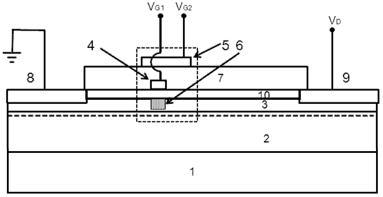
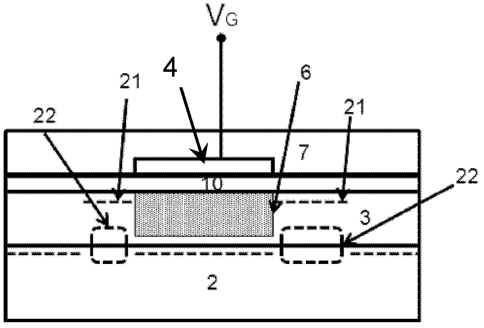
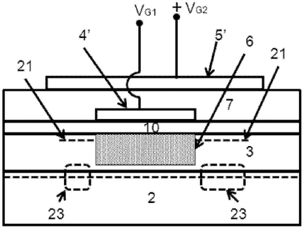
[0021] refer to Figure 2a , the reason for the current collapse phenomenon of ordinary enhanced MISHEMT devices (taking AlGaN / GaN devices as an example) is that in the off state of the device, negative charges will be accumulated at the interface between the AlGaN layer 3 and the first dielectric layer 10 on both sides of the gate metal 4 , forming an interface negative charge accumulation region 21 , due to electrostatic induction, these negative charges will reduce or even completely deplete the two-dimensional electron gas in the lower channel region, forming a channel depletion region 22 . When the gate voltage rises and the device transitions from the off state to the on state, the two-dimensional electron gas under the gate rises under the control of the gate voltage, and the channel under the gate is turned on, but the negative charges in the interface charge accumulation region are relatively low The deep energy level cannot be released in time, so the two-dimensional...


PUM


Abstract

The invention discloses a III-nitride enhanced-mode metal-insulator-semiconductor high electron mobility transistor (MISHEMT) device, which comprises a source electrode, a drain electrode, a primary gate, a secondary gate, a first dielectric layer, a second dielectric layer and a heterostructure, wherein the source and drain electrodes are electrically connected through a two-dimensional electron gas which is formed in the heterostructure; the heterostructure comprises a first semiconductor and a second semiconductor; the first semiconductor is arranged between the source and drain electrodes; the second semiconductor is formed on the surface of the first semiconductor, and has a band gap which is wider than the first semiconductor; the first dielectric layer is arranged on the surface of the second semiconductor; the second dielectric layer is arranged on the surfaces of the first dielectric layer and the primary gate; the primary gate is arranged on the side, close to the source electrode, of the surface of the first dielectric layer, and forms a metal insulator semiconductor (MIS) structure with the first dielectric layer and the second semiconductor; a plasma treatment area is formed in a local area of the second semiconductor below the primary gate; the secondary gate is formed on the surface of the second dielectric layer; at least one side edge of the secondary gate is extended towards the source electrode or the drain electrode; and simultaneously, the orthographic projection of the secondary gate is overlapped with both side edges of the primary gate. By the III-nitride enhanced-mode MISHEMT device, 'current collapse' can be radically effectively inhibited.

Description

technical field [0001] The present invention relates to an enhanced high electron mobility transistor (Enhancement-mode Metal-Insulator-Semiconductor High Electron Mobility Transistor, E-Mode MISHEMT), in particular to a Group III nitride enhanced MISHEMT device. Background technique [0002] When MISHEMT devices use group III nitride semiconductors, due to piezoelectric polarization and spontaneous polarization effects, a high-concentration two-dimensional electron gas can be formed on a heterostructure (such as AlGaN / GaN). In addition, MISHEMT devices use group III nitride semiconductors, which can obtain high insulation breakdown electric field strength and good high temperature resistance characteristics. MISHEMTs with heterostructured group III nitride semiconductors can be used not only as high-frequency devices, but also as high-voltage, high-current power switching devices. When applied to high-power switching circuits, for the sake of simple circuit design and safe...

Claims


Application Information

Patent Timeline
Patent Type & Authority Patents(China)
IPC IPC(8): H01L29/778H01L29/423
Inventor 蔡勇于国浩董志华王越张宝顺
Owner SUZHOU INST OF NANO TECH & NANO BIONICS CHINESE ACEDEMY OF SCI
Why Eureka
Try Eureka