Deep ultraviolet light-emitting element and preparation method thereof

A light-emitting element, deep ultraviolet technology, applied in electrical components, chemical instruments and methods, semiconductor devices, etc., can solve the problems of aging light attenuation, large concentration difference, uneven distribution, etc., to improve luminous efficiency and intensity, reduce aging Light attenuation, effects that improve consistency and uniformity

Active Publication Date: 2021-09-17
XIAMEN SILAN ADVANCED COMPOUND SEMICON CO LTD +1
View PDF9 Cites 2 Cited by
  • Summary
  • Abstract
  • Description
  • Claims
  • Application Information

AI Technical Summary

Problems solved by technology

The large difference in concentration and uneven distribution of electrons and holes in deep ultraviolet light-emitting elements are important reasons for their luminous efficiency to be generally lower than 5%.
In addition, the distance between the Si-doped layer of the quantum well layer and the Mg-doped layer of the p-type semiconductor layer is too close, which will easily lead to the migration and diffusion of Mg and Si elements under high temperature or long-term use and mix, thus causing aging light attenuation.

Method used


Image

  • Deep ultraviolet light-emitting element and preparation method thereof
  • Deep ultraviolet light-emitting element and preparation method thereof

Examples


Embodiment Construction

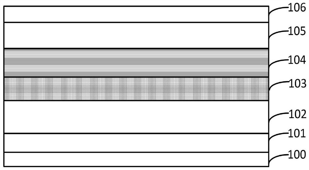
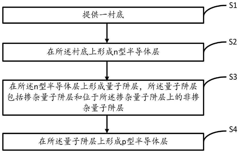
[0055] The quantum well layer of the existing deep ultraviolet light-emitting element is a single-group quantum well structure. Due to the different doping and ionization efficiency of electrons and holes in the deep ultraviolet light-emitting element, the distribution of electrons and holes in the quantum well layer is extremely polar. Non-uniform, and the concentration difference is large, and this phenomenon is more serious with the increase of Al composition in the p-type semiconductor layer, and the large concentration difference and non-uniform distribution of electrons and holes in the deep ultraviolet light-emitting element lead to its general luminous efficiency. Important reasons for less than 5%. In addition, the distance between the Si-doped layer of the quantum well layer and the Mg-doped layer of the p-type semiconductor layer is too close, which will easily lead to element migration and diffusion of Mg and Si under high temperature or long-term use, resulting in ...


PUM

PropertyMeasurementUnit
thicknessaaaaaaaaaa
thicknessaaaaaaaaaa

Abstract

The invention provides a deep ultraviolet light-emitting element and a preparation method thereof. The deep ultraviolet light-emitting element sequentially comprises a substrate, an n-type semiconductor layer, a quantum well layer and a p-type semiconductor layer from bottom to top, wherein the quantum well layer comprises a doped quantum well layer and a non-doped quantum well layer located on the doped quantum well layer. By arranging the double quantum well structures, the luminous efficiency and intensity are improved, and due to the fact that the non-doped quantum well layer is arranged between the doped quantum well layer and the p-type semiconductor layer, the phenomenon of luminous decay caused by migration of Mg and Si under the condition of high temperature or long-term use can be reduced, and the luminous decay within 1000 hours is reduced from 30% to 10% or below.

Description

technical field [0001] The invention relates to the technical field of semiconductors, in particular to a deep ultraviolet light-emitting element and a preparation method thereof. Background technique [0002] The deep ultraviolet light-emitting element has a wavelength range of 200-300nm. The deep ultraviolet light emitted can interrupt the DNA or RNA of viruses and bacteria, and directly kill viruses and bacteria. It can be widely used in air purification, tap water sterilization, household air conditioning sterilization, Auto air conditioner sterilization and other sterilization fields. [0003] The p-type semiconductor layer of the deep ultraviolet light emitting element uses AlGaN with high Al composition. As the Al composition increases, the doping and ionization efficiency of Mg decreases, resulting in the hole concentration of the deep ultraviolet light emitting element generally lower than 1E17 cm -2 , while the n-type semiconductor layer is doped with Si, the dopi...

Claims


Application Information

Patent Timeline
Patent Type & Authority Applications(China)
IPC IPC(8): H01L33/06H01L33/00A61L2/10A61L9/20C02F1/32
CPCH01L33/06H01L33/0075H01L33/007A61L9/20A61L2/10C02F1/325C02F2303/04
Inventor 郑锦坚高默然毕京锋范伟宏曾家明张成军
Owner XIAMEN SILAN ADVANCED COMPOUND SEMICON CO LTD
Why Eureka
Try Eureka