Micro light-emitting diode display production detection method and display thereof
A micro-light-emitting diode, production detection technology, applied in static indicators, instruments, etc., can solve the problems affecting the production efficiency of displays, obstacles to rapid mass production of displays, etc., to ensure rapid mass production, improve production efficiency, and reduce complexity. Effect
- Summary
- Abstract
- Description
- Claims
- Application Information
AI Technical Summary
Problems solved by technology
Method used
Image
Examples
Embodiment 1
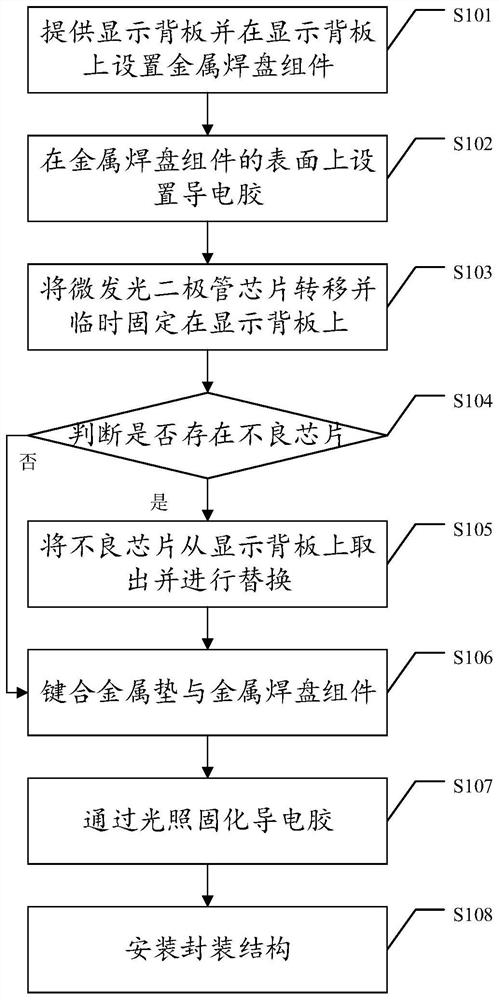
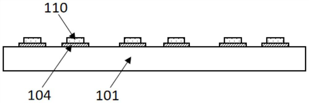
[0053] The production and detection method of a micro-light-emitting diode display of the present invention is described in detail below by taking a production and detection method of a flip-chip display as an example. Please refer to Figure 1 to Figure 7 , which includes:
[0054] S101. Provide a display backplane and set a metal pad assembly on the display backplane
[0055]Provide a display backplane 101, the display backplane 101 is a thin film transistor (TFT, Thin FilmTransistor) backplane; and set more than two metal pad components 104 on the display backplane 101, wherein each metal Pad assembly 104 is made up of two metal pads, which are positive electrode pads and negative electrode pads respectively; the metal pads are made of titanium Ti, gold Au, tin Sn, copper Cu, indium In, silver Ag, platinum Pt, One or several metals in chromium Cr and nickel Ni are formed after coating, exposure, development, etching and stripping.
[0056] S102. Disposing conductive glue ...
Embodiment 2
[0071] Taking the production and detection method of a vertical structure chip display as an example below, a kind of micro light-emitting diode display production and detection method of the present invention is described in detail, please refer to Figure 8 to Figure 15 , which includes:
[0072] S201. Provide a display backplane and set a metal pad assembly on the display backplane
[0073] A display backplane 101 is provided, and the display backplane 101 is a thin film transistor backplane; and more than two metal pad assemblies 104 are arranged on the display backplane 101, wherein each metal pad assembly 104 consists of A metal pad; the metal pad is made of one or more metals in titanium Ti, gold Au, tin Sn, copper Cu, indium In, silver Ag, platinum Pt, chromium Cr, nickel Ni through coating, exposure , development, etching, and stripping.
[0074] S202. Disposing conductive glue on the surface of the metal pad assembly
[0075] The surface of the metal pad is coated...
Embodiment 3
[0091] A micro light-emitting diode display of the present invention is described in detail below with an embodiment of a flip-chip display, please refer to Figure 16 , which includes:
[0092]The display backplane 101 is provided with more than one set of metal pad assemblies 104 on the display backplane 101, and each set of metal pad assemblies 104 is composed of two metal pads, which are positive pads and negative pads respectively , and the metal pad assembly 104 is formed by patterning one or more metals of titanium Ti, gold Au, tin Sn, copper Cu, indium In, silver Ag, platinum Pt, chromium Cr, nickel Ni . And the surfaces of the positive electrode pad and the negative electrode pad are all connected to the metal pad 105 at the lower end of the micro-light emitting diode chip 103 through the conductive glue 110; wherein, the conductive glue 110 is a photocurable conductive glue, and the main body of the conductive glue 110 includes : Epoxy resin, silicone, and its main...
PUM
 Abstract
Description
Claims
Application Information
 - R&D
- Intellectual Property
- Life Sciences
- Materials
- Tech Scout
- Unparalleled Data Quality
- Higher Quality Content
- 60% Fewer Hallucinations
Browse by: Latest US Patents, China's latest patents, Technical Efficacy Thesaurus, Application Domain, Technology Topic, Popular Technical Reports.
© 2025 PatSnap. All rights reserved.Legal|Privacy policy|Modern Slavery Act Transparency Statement|Sitemap|About US| Contact US: help@patsnap.com


