
Design method of radio frequency circuit layer structure

A design method and circuit layer technology, applied in the direction of circuit devices, printed circuits, printed circuit manufacturing, etc., can solve problems such as large differences in performance indicators and circuit systems that cannot work normally, so as to improve reliability, solve electromagnetic interference problems, The effect of improving the anti-interference ability

Inactive Publication Date: 2021-10-01
深圳市宏联电路有限公司
View PDF2 Cites 0 Cited by
  • Summary
  • Abstract
  • Description
  • Claims
  • Application Information

AI Technical Summary

Problems solved by technology

[0004] However, in the same circuit, different PCB design structures will lead to great differences in its performance indicators. Once the electromagnetic interference signal is not handled properly, it may cause the entire circuit system to fail to work normally.

Method used


Image

  • Design method of radio frequency circuit layer structure
  • Design method of radio frequency circuit layer structure
  • Design method of radio frequency circuit layer structure

Examples


Embodiment Construction

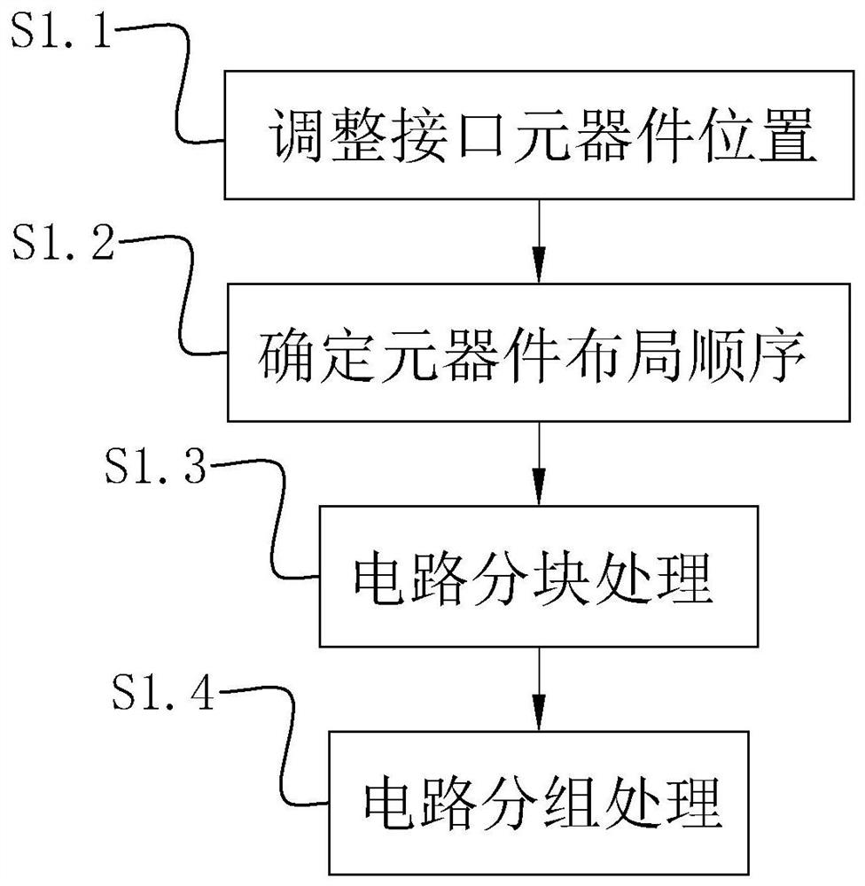
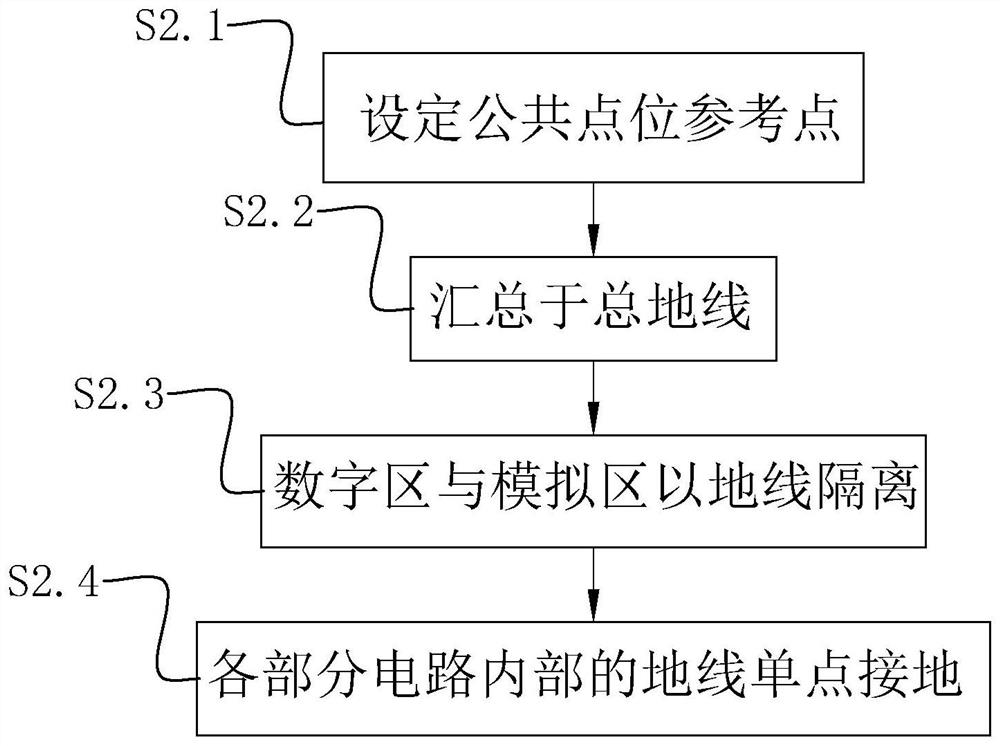
[0044] The following is attached Figure 1-3 The application is described in further detail.

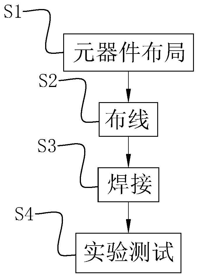
[0045] The embodiment of the present application discloses a method for designing a radio frequency circuit layer structure. refer to figure 1 , a method for designing a radio frequency circuit layer structure, comprising the following steps:

[0046] S1. Component layout.

[0047] Wherein, the components are arranged in the same direction on the circuit board. Specifically, the general principle of layout is that the components should be arranged in the same direction as possible, and the phenomenon of poor soldering can be reduced or even avoided by selecting the direction in which the PCB enters the tin melting system.

[0048] In addition, there is at least 0.5mm spacing between the components to meet the tin melting requirements of the components. If the space of the PCB board allows, the spacing of the components should be set to be greater than 0.5mm.

[0049] refer to ...


PUM


Abstract

The invention relates to a design method of a radio frequency circuit layer structure, belonging to the technical field of wireless radio frequency circuit technology. The design method comprises the following steps: S1, component layout: arranging components on a circuit board in the same direction; S2, wiring: performing low-density wiring designing, and keeping the thickness of signal wiring consistent; S3, welding; and S4, experimental testing. According to the invention, the reliability of a radio frequency circuit design is improved, the problem of electromagnetic interference is solved, and the purpose of electromagnetic compatibility is achieved.

Description

technical field [0001] The present application relates to the technical field of wireless radio frequency circuit technology, in particular to a design method of a radio frequency circuit layer structure. Background technique [0002] Radio frequency is a non-contact automatic identification technology that emerged in the 1990s. Compared with traditional magnetic card and IC card technology, radio frequency technology has the characteristics of non-contact, fast reading speed, and no wear and tear. Wireless radio frequency technology performs non-contact two-way data transmission between the reader and the radio frequency card to achieve the purpose of target identification and data exchange. [0003] In the current application of wireless radio frequency circuit technology, the performance index of the radio frequency circuit directly affects the quality of the entire product. The anti-interference design of the printed circuit board (PCB) of the radio frequency circuit c...

Claims


Application Information

Patent Timeline
Patent Type & Authority Applications(China)
IPC IPC(8): H05K1/02H05K3/00
CPCH05K1/0216H05K1/0218H05K3/0002H05K3/00
Inventor 王建业甘颖燕陈丽曹爱华盛国利
Owner 深圳市宏联电路有限公司
Learn More