Storage device amd method for forming storage

A memory and storage line technology, applied in static memory, digital memory information, manufacturing/processing of electromagnetic devices, etc., to achieve the effects of reduced write current, reduced distance, and reduced cross-interference

Active Publication Date: 2006-09-06
TAIWAN SEMICON MFG CO LTD
View PDF1 Cites 2 Cited by
  • Summary
  • Abstract
  • Description
  • Claims
  • Application Information

AI Technical Summary

Problems solved by technology

But since the top write line is used to generate a magnetic field to write to the MTJ, this write line needs to be close to the MTJ

Method used


Image

  • Storage device amd method for forming storage
  • Storage device amd method for forming storage
  • Storage device amd method for forming storage

Examples


Embodiment Construction

[0029] In order to make the above objects, features and advantages of the present invention more comprehensible, a preferred embodiment will be described in detail below together with the accompanying drawings.

[0030] Figure 4 Shown is a cross-sectional view of an early stage of a process. Such as Figure 4 As shown, the device includes a substrate 110 having a dielectric layer 112 formed thereon, a series of conductive lines 114 - 117 , an insulating layer (spacer layer) 122 , an electrode layer 124 and a magnetoresistive layer 126 .

[0031] The substrate 110 may be a semiconductor substrate, such as a P-type silicon wafer with a lattice surface . The substrate 110 also includes any other suitable semiconductor material, such as gallium arsenide (GaAs), indium phosphide (InP), silicon carbide (SiC) or silicon / germanium (Si / Ge). The substrate 110 also includes active devices or circuits formed in front-end-of-line (FEOL), not shown here.

[0032] In one embodiment, the...


PUM


Abstract

An improved magnetoresistive memory device has a reduced distance between the magnetic memory element and a conductive memory line used for writing to the magnetic memory element. The reduced distance is facilitated by forming the improved magnetoresistive memory device according to a method that includes forming a mask over the magnetoresistive memory element and forming an insulating layer over the mask layer, then removing portions of the insulating layer using a planarization process. A conductive via can then be formed in the mask layer, for example using a damascene process. The conductive memory line can then be formed over the mask layer and conductive via.

Description

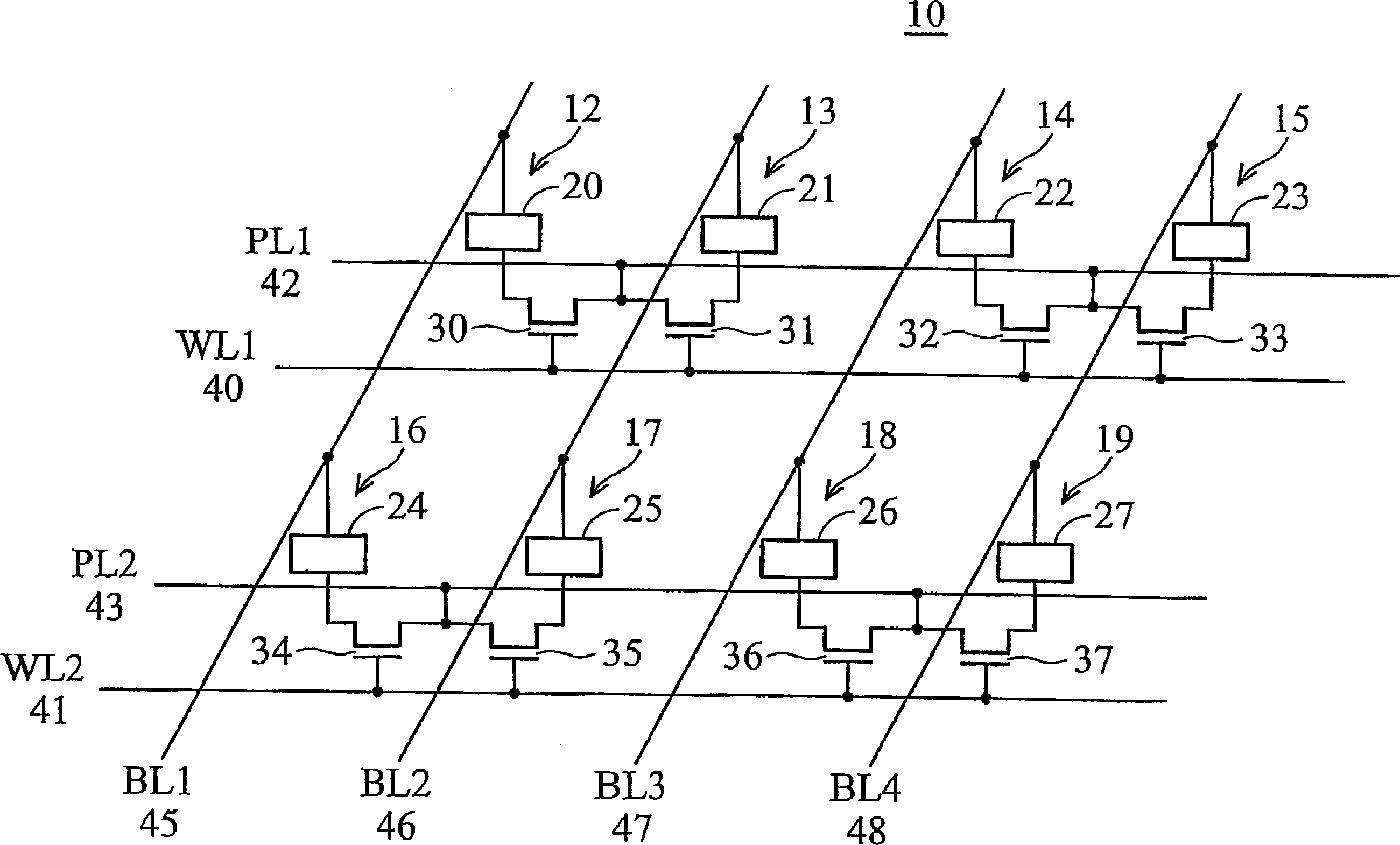
technical field [0001] The present invention relates to a semiconductor storage device; especially a semiconductor storage device using a magnetoresistive structure to store data. Background technique [0002] Magnetic random access memory (MRAM) is a type of non-volatile memory that uses magnetism instead of electricity to store data. figure 1 is a partial schematic diagram showing a MRAM array 10 . The MRAM array 10 includes a plurality of memory cells 12-19, and a series of wires 40-48. Each memory cell 12-19 includes a magnetoresistive (MR) memory element 20-27 and a transistor 30-37. figure 1 The structure shown is also referred to as a 1T1MTJ (one transistor, one MTJ) structure. [0003] Such as figure 1 As shown, the transistors 30-33 are coupled to each other through a word line WL140, and the transistors 34-37 are coupled to each other through a word line WL241, wherein the word lines 40 and 41 form the gates of the transistors 30-37. The transistors 34-37 are ...

Claims


Application Information

Patent Timeline
Patent Type & Authority Applications(China)
IPC IPC(8): H01L21/82H01L27/22H01L43/00G11C11/02
CPCH01L27/228H01L43/12H10B61/22H10N50/01
Inventor 刘源鸿吴志达赵兰璘杜友伦林文钦蔡嘉雄
Owner TAIWAN SEMICON MFG CO LTD
Why Eureka
Try Eureka