

High-strength bonding structure with special groove and preparation method of high-strength bonding structure
A bonding structure and high-strength technology, applied in semiconductor/solid-state device manufacturing, electrical components, electrical solid-state devices, etc., can solve problems such as high production cost, chip failure, solder overflow, etc., to improve bonding strength and prevent phase Short-circuit between adjacent metals and prevent solder overflow
- Summary
- Abstract
- Description
- Claims
- Application Information
AI Technical Summary
Problems solved by technology
Method used
Image

Examples
preparation example Construction
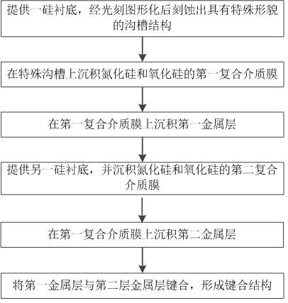
[0029] refer to figure 1 , the preparation method of the high-strength bonding structure comprises the following steps:
[0030] Step 1, provide a silicon substrate material 1, photolithographic patterning is carried out on the substrate, and a groove structure 2 with a special shape is produced after dry etching and deglue, and the groove structure 2 is a rectangular groove Groove array 41 is made up of rectangular annular sealing groove 42, such as Figure 5 shown;
[0031] In step 2, a composite dielectric film of silicon nitride and silicon oxide is fabricated on the trench structure 2 by means of plasma-enhanced chemical vapor deposition, and the composite dielectric layer 3 is obtained after photolithographic patterning and dry etching. 3 After metal deposition, photolithographic patterning, and wet etching, the first metal layer 4 used for bonding is obtained, such as figure 2 shown;
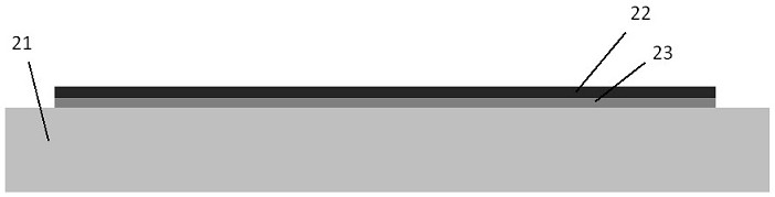
[0032] Step 4, providing another silicon substrate material 21, on which a compo...
Embodiment 1
[0036] The preparation method of the groove-containing high-strength bonding structure of this embodiment includes the following steps:
[0037] Step 1, provide a silicon substrate material 1, the silicon substrate material is (100) type silicon, after photolithographic patterning and dry etching on the substrate, a groove structure 2 with a special shape is produced, the groove The groove structure 2 is composed of a rectangular groove array 41 and a rectangular annular sealing groove 42, wherein the length of the rectangular groove is 300um, the width is 5um, the interval between adjacent grooves is 15um, and the groove depth is 3um; the width of the rectangular annular sealing groove is 10um, 15um away from the rectangular trench array;
[0038] Step 2, successively deposit composite dielectric film layers 3 of silicon nitride and silicon oxide on the special trench structure 2. The composite dielectric film is formed by the growth method of plasma enhanced chemical vapor d...
Embodiment 2
[0042] The preparation method of the groove-containing high-strength bonding structure of this embodiment includes the following steps:
[0043]Step 1, provide a silicon substrate material 1, the silicon substrate material is (100) type silicon, after photolithographic patterning and dry etching on the substrate, a groove structure 2 with a special shape is produced, the groove The groove structure 2 is composed of a rectangular groove array 41 and a rectangular annular sealing groove 42, wherein the length of the rectangular groove is 500um, the width is 10um, the interval between adjacent grooves is 15um, and the groove depth is 2um; the width of the rectangular annular sealing groove is 15um, 30um away from the rectangular trench array;
[0044] Step 2, successively deposit composite dielectric film layers 3 of silicon nitride and silicon oxide on the special trench structure 2. The composite dielectric film is formed by the growth method of plasma enhanced chemical vapor d...
PUM
| Property | Measurement | Unit |
|---|---|---|
| thickness | aaaaa | aaaaa |
| thickness | aaaaa | aaaaa |
Abstract
Description
Claims
Application Information