Supercharge Your Innovation With Domain-Expert AI Agents!

Manufacturing method of transistor, transistor, basic memory cell and dynamic random access memory

A manufacturing method and technology of transistors, which are applied in the fields of transistors, semiconductor/solid-state device manufacturing, and electric solid-state devices, etc., can solve the problems of difficult control, high process complexity, and high failure rate, and achieve flexible structure, improved performance, and increased quantity. Effect

Pending Publication Date: 2021-10-19
ICLEAGUE TECH CO LTD
View PDF0 Cites 0 Cited by
  • Summary
  • Abstract
  • Description
  • Claims
  • Application Information

AI Technical Summary

Problems solved by technology

[0003] Since the bit line and the storage device of the dynamic random access memory are connected to one of the source / drain respectively, the transistors of these two structures are used to make the memory, and the bit line and the storage device capacitor are located on the same side of the gate. In terms of processing technology, they are all located on the same side of the wafer, so that the overall process complexity is high, especially for photolithography and related processes, which have extremely high requirements, process control is difficult, and the failure rate is high.

Method used


Image

  • Manufacturing method of transistor, transistor, basic memory cell and dynamic random access memory
  • Manufacturing method of transistor, transistor, basic memory cell and dynamic random access memory
  • Manufacturing method of transistor, transistor, basic memory cell and dynamic random access memory

Examples


Embodiment Construction

[0016] The specific implementation methods of the manufacturing method of the transistor, the transistor, the basic storage unit, and the dynamic random access memory provided by the present invention will be described in detail below with reference to the accompanying drawings.

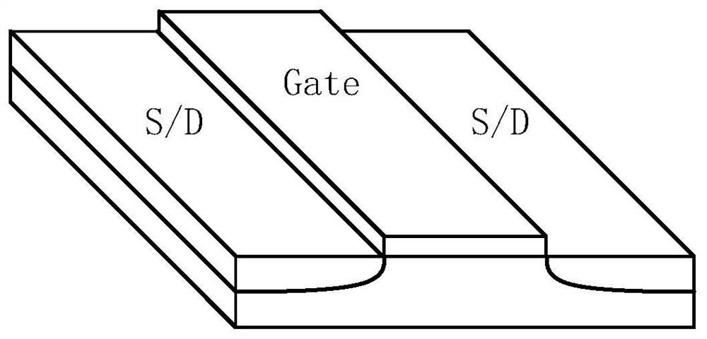
[0017] attached image 3 Shown is a schematic diagram of the implementation steps of the specific embodiment of the transistor manufacturing method of the present invention, including: Step S30, forming a conductive channel, the conductive channel includes a columnar body and ends on both sides, and at least one of the ends is protruding setting; step S31, forming a gate insulating layer surrounding the columnar body, and exposing the ends on both sides of the conductive channel; step S32, forming a gate electrode surrounding the gate insulating layer; step S33, in the The ends on both sides of the conductive channel form source and drain electrodes.

[0018] attached Figure 4A to attach Figure ...


PUM


Abstract

The invention provides a manufacturing method of a transistor, the transistor, a basic memory cell and a dynamic random access memory. The method comprises the following steps of forming a conductive channel, wherein the conductive channel comprises a columnar body and end portions on the two sides, and at least one of the end portions is arranged in a protruding mode, forming a gate insulating layer surrounding the columnar body, and exposing the end portions of the two sides of the conductive channel, forming a gate electrode surrounding the gate insulating layer, and forming a source electrode and a drain electrode at the end portions of the two sides of the conductive channel. The transistor is improved from a horizontal transistor in the prior art to a vertical transistor, so that the area occupied by a single transistor in the horizontal direction is reduced, the number of transistors in unit area is increased, and the density of the transistors is improved.

Description

technical field [0001] The invention relates to the field of semiconductor technology, in particular to a method for manufacturing a transistor, a transistor, a basic storage unit, and a dynamic random access memory. Background technique [0002] Basic unit of dynamic random access memory as attached Figure 1A shown, and by attaching Figure 1B The array structure shown forms a memory. The basic unit is often referred to as a 1T1C structure. Among them, 1T, the transistor, mainly has attached Figure 2A The planar transistor and attached Figure 2B Two structures of buried channel array transistors are shown. For the transistors of these two structures, the source and the drain are distributed on both sides of the horizontal plane direction of the gate, so that the area occupied by the transistor in the horizontal direction is relatively large. [0003] Because the bit line and the storage device of the dynamic random access memory are connected to one of the source / dr...

Claims


Application Information

Patent Timeline
Patent Type & Authority Applications(China)
IPC IPC(8): H01L29/78H01L27/108H01L21/336H10B12/00
CPCH01L29/785H01L29/66795H10B12/30
Inventor 华文宇薛迎飞
Owner ICLEAGUE TECH CO LTD
Features
  • R&D
  • Intellectual Property
  • Life Sciences
  • Materials
  • Tech Scout
  • Unparalleled Data Quality
  • Higher Quality Content
  • 60% Fewer Hallucinations
Learn More