

High-thermal-conductivity silicon carbide device packaging structure and method
A device packaging, high thermal conductivity technology, applied in the direction of semiconductor devices, semiconductor/solid-state device manufacturing, semiconductor/solid-state device components, etc., can solve problems such as the stability of the unfavorable silicon carbide device structure, normal use, and increased heat generation. , to achieve good cooling effect and reduce conduction loss
- Summary
- Abstract
- Description
- Claims
- Application Information
AI Technical Summary
Problems solved by technology
Method used
Image

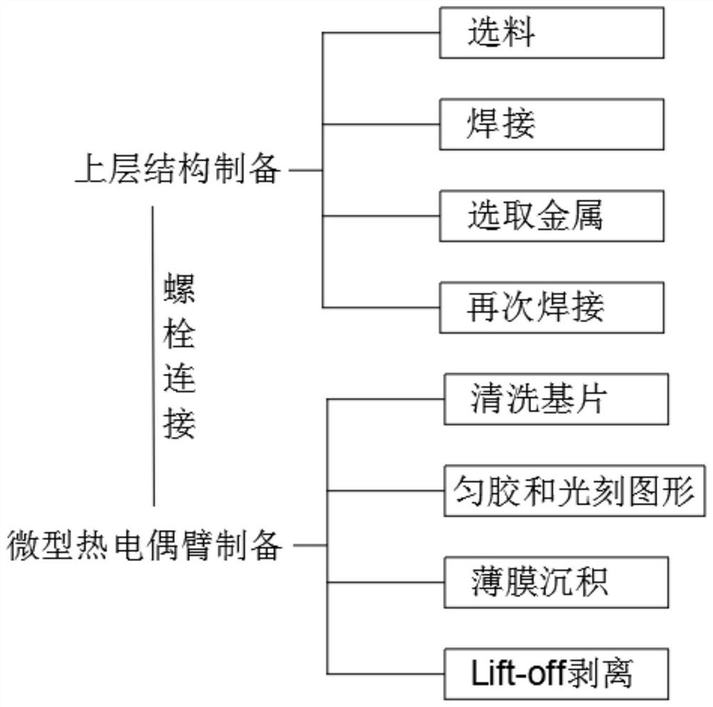
Examples
Embodiment 1
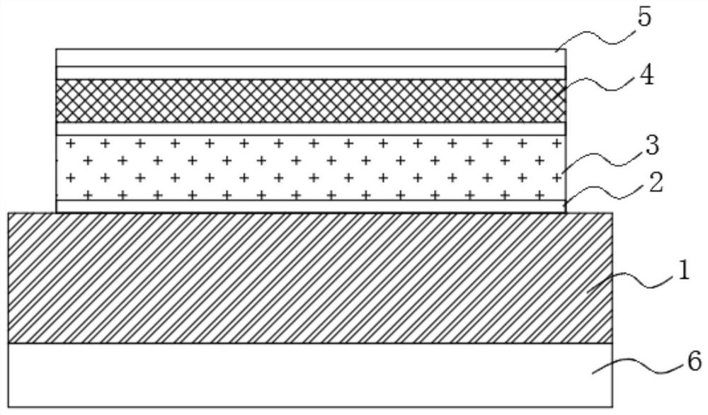
[0025] Embodiment one, by Figure 1-2 Provided, the present invention provides a high thermal conductivity silicon carbide device packaging structure and method, including a heat sink 1, an adhesive layer 2, a metal layer 3, an insulating substrate 4, a circuit layer 5 and a miniature thermocouple arm 6, the thermal The surface of the sink 1 is connected to the metal layer 3 through the bonding layer 2, the surface of the metal layer 3 is connected to the insulating substrate 4 through the bonding layer 2, the surface of the insulating substrate 4 is connected to the circuit layer 5 through the bonding layer 2, and the heat sink 1 A miniature thermocouple arm 6 is mounted on the bottom end of the bottom end by bolts.
[0026] The insulating substrate 4 is one or more of aluminum nitride ceramic materials, alumina ceramic materials or silicon carbide ceramic materials.
[0027] The bonding layer 2 adopts active metal brazing material.
[0028] A high thermal conductivity sili...
PUM
| Property | Measurement | Unit |
|---|---|---|
| thickness | aaaaa | aaaaa |
| thickness | aaaaa | aaaaa |
| thickness | aaaaa | aaaaa |
Abstract
Description
Claims
Application Information