Semiconductor structure and forming method thereof

A technology of semiconductor and pseudo-gate structure, which is used in semiconductor devices, semiconductor/solid-state device manufacturing, electrical components, etc., can solve the problem that the performance of semiconductor devices needs to be improved, and achieve the goal of improving short-channel effect, improving performance and reducing impact. Effect

Pending Publication Date: 2021-10-22
SEMICON MFG INT (SHANGHAI) CORP +1
View PDF0 Cites 0 Cited by
  • Summary
  • Abstract
  • Description
  • Claims
  • Application Information

AI Technical Summary

Problems solved by technology

[0004] However, the performance of semiconductor de...

Method used


Image

  • Semiconductor structure and forming method thereof
  • Semiconductor structure and forming method thereof
  • Semiconductor structure and forming method thereof

Examples


Embodiment Construction

[0039] As mentioned in the background, existing semiconductor structures perform poorly.

[0040] The reasons for the poor performance of the semiconductor structure will be described in detail below in conjunction with the accompanying drawings. Figure 1 to Figure 4 It is a structural schematic diagram of each step of a method for forming a semiconductor structure.

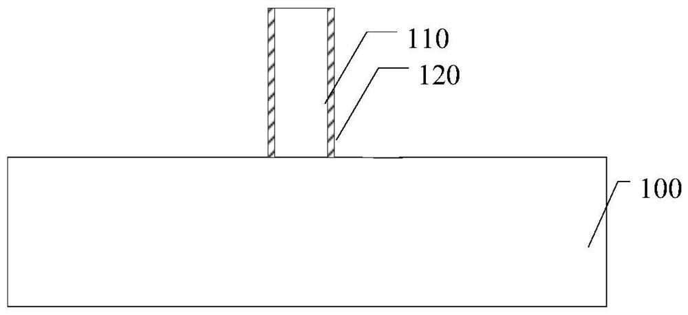
[0041] Please refer to figure 1 , providing a substrate 100, the surface of the substrate 100 has a dummy gate structure 110, and the dummy gate structure 110 has sidewalls 120 on both sides.

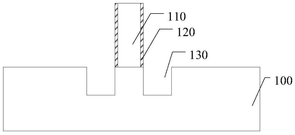
[0042] Please refer to figure 2 , forming source and drain openings 130 in the substrate 100 on both sides of the dummy gate structure 110 and the spacer 120 .

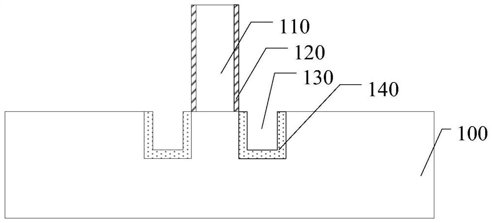
[0043] Please refer to image 3 , forming a first stress layer 140 on the bottom and sidewall surfaces of the source-drain opening 130 .

[0044] Please refer to Figure 4 , forming a second stress layer 150 on the surface of the first stress layer 140 , a...


PUM


Abstract

The invention discloses a semiconductor structure and a forming method thereof. The semiconductor structure comprises a substrate of which the surface is provided with a dummy gate structure, source-drain openings which are respectively positioned at two sides of the dummy gate structure in the substrate, a first stress layer which is positioned on the side walls of the source-drain openings, a second stress layer which is located at the bottoms of the source-drain openings and on the first stress layer, wherein the source-drain openings are filled with the second stress layer, and the stress of the first stress layer is smaller than that of the second stress layer. The first stress layer is only located on the side walls of the source-drain openings and occupies a small space of the source-drain openings, so that the size of the second stress layer formed in the source-drain openings is large, and the stress of the second stress layer on a channel is further improved. Meanwhile, the first stress layer can relieve the interface defect between the substrate and the second stress layer, so that the influence on the channel can be reduced, and the short channel effect is improved.

Description

technical field [0001] The invention relates to the technical field of semiconductor manufacturing, in particular to a semiconductor structure and a forming method thereof. Background technique [0002] With the rapid development of integrated circuit manufacturing technology, the size of semiconductor devices in the integrated circuit is continuously reduced, so that the operation speed of the entire integrated circuit will be effectively improved. [0003] In VLSI, stress is usually formed on the transistor to increase the carrier mobility of the transistor to increase the driving current of the transistor. [0004] However, the performance of semiconductor devices formed in the prior art needs to be improved. Contents of the invention [0005] The technical problem solved by the present invention is to provide a semiconductor structure and its forming method, so as to improve the performance of the formed semiconductor structure. [0006] In order to solve the above t...

Claims


Application Information

Patent Timeline
IPC IPC(8): H01L29/78H01L21/336
CPCH01L29/785H01L29/66795H01L29/66545H01L29/7848H01L29/165H01L29/0619H01L29/66553
Inventor 赵猛
Owner SEMICON MFG INT (SHANGHAI) CORP
Why Eureka
Try Eureka