Cross beam film stress concentration micro-pressure sensor chip and preparation method thereof

A technology of micro-pressure sensor and stress concentration, which is applied in the measurement of the property force of piezoelectric resistance materials, the measurement of fluid pressure by changing the ohmic resistance, ion implantation plating, etc. Accurate measurement, low sensitivity and other problems, to achieve high dynamic performance, improve sensitivity, high sensitivity effect

Active Publication Date: 2021-10-26
陕西省计量科学研究院 +1
View PDF8 Cites 5 Cited by
  • Summary
  • Abstract
  • Description
  • Claims
  • Application Information

AI Technical Summary

Problems solved by technology

[0006] At present, the minimum range of the relatively mature MEMS piezoresistive micro-pressure sensor products on the market is mostly on the kPa level, and the only Pa level products have low sensitivity, and poor nonlinear and dynamic performance, making it difficult to achieve accurate measurement

Method used


Image

  • Cross beam film stress concentration micro-pressure sensor chip and preparation method thereof
  • Cross beam film stress concentration micro-pressure sensor chip and preparation method thereof
  • Cross beam film stress concentration micro-pressure sensor chip and preparation method thereof

Examples


Embodiment Construction

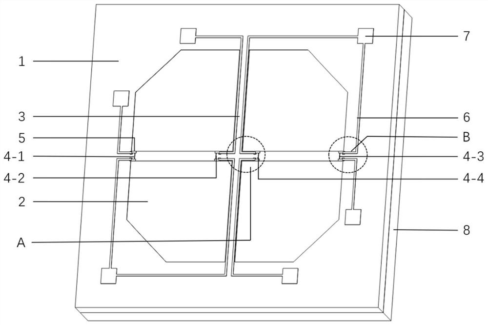
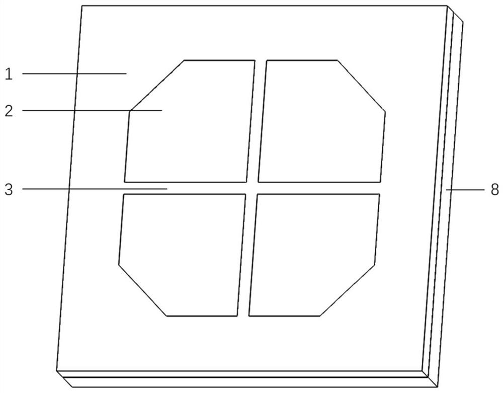
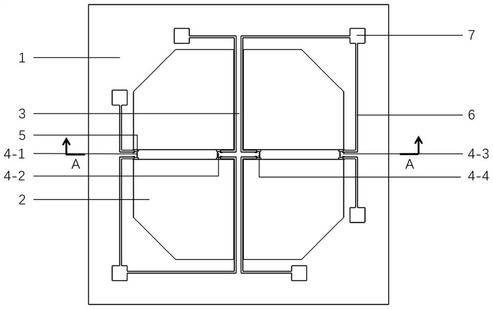
[0054] In order to make the purpose and technical solution of the present invention clearer and easier to understand. The present invention will be further described in detail below in conjunction with the drawings and embodiments. The specific embodiments described here are only used to explain the present invention, not to limit the present invention.

[0055] In describing the present invention, it should be understood that the terms "center", "longitudinal", "transverse", "upper", "lower", "front", "rear", "left", "right", " The orientations or positional relationships indicated by "vertical", "horizontal", "top", "bottom", "inner" and "outer" are based on the orientations or positional relationships shown in the drawings, and are only for the convenience of describing the present invention and Simplified descriptions, rather than indicating or implying that the device or element referred to must have a particular orientation, be constructed and operate in a particular ori...


PUM

PropertyMeasurementUnit
widthaaaaaaaaaa
Sensitivityaaaaaaaaaa

Abstract

The invention discloses a cross beam film stress concentration micro-pressure sensor chip and a preparation method thereof. The sensor chip comprises a pressure-bearing film, a silicon substrate, a piezoresistor strip, a metal lead, an anti-overload glass substrate and the like. According to the specific structure, the back face of a silicon substrate is etched to form a pressure-bearing film and a peninsular and island structure, and four diamond-shaped areas are etched on the front face of the silicon substrate to form a cross beam. Stress concentration areas are formed on the front face of the chip corresponding to gaps between islands adjacent to a chip back cavity and between the islands and peninsula, the four piezoresistor strips are arranged on the stress concentration areas, and the piezoresistor strips are connected to form a Wheatstone bridge through heavily-doped ohmic contact areas, metal leads and metal bonding pads. The existence of the cross beam can further improve the stress concentration effect at the piezoresistor strip.

Description

technical field [0001] The invention belongs to the technical field of micro-electromechanical sensors, and in particular relates to a cross-beam membrane stress concentration micro-pressure sensor chip and a preparation method thereof. Background technique [0002] With the development of MEMS technology, MEMS micro-pressure sensors have been widely used in aerospace, food industry, smart home, biomedical and other fields; with the rapid development of various fields, higher requirements have been put forward for the performance and volume of sensors. Requirements, especially in the field of biomedicine, there is an urgent need for MEMS micro-pressure sensors with stable performance, high dynamic performance, high sensitivity, and high linearity to guarantee. [0003] According to different measurement principles, MEMS micro-pressure sensors are mainly divided into piezoresistive, piezoelectric, capacitive, and resonant. Compared with MEMS micro-pressure sensors of other p...

Claims


Application Information

Patent Timeline
Patent Type & Authority Applications(China)
IPC IPC(8): G01L1/18G01L9/06C23C14/34C23C14/16C23C14/58C23C16/40C23C16/50C23C16/56
CPCG01L1/18G01L9/06C23C14/34C23C14/165C23C14/5873C23C16/402C23C16/50C23C16/56Y02P70/50
Inventor 王鸿雁李学琛关卫军吴永顺魏于昆山涛王爱华付磊赵立波韩香广皇咪咪徐廷中杨萍王李陈翠兰罗国希王永录蒋庄德
Owner 陕西省计量科学研究院
Why Eureka
Try Eureka