A kind of pim device and manufacturing method thereof

A technology of devices and gates, which is applied in the field of PIM devices and its manufacturing, can solve the problems of poor conduction capacity, slow production efficiency, and high process difficulty, and achieve the effects of clear connection points, reduced production error rate, and simplified circuit structure

Active Publication Date: 2022-04-01
乐山希尔电子股份有限公司 +1
View PDF0 Cites 0 Cited by
  • Summary
  • Abstract
  • Description
  • Claims
  • Application Information

AI Technical Summary

Problems solved by technology

[0003] 1. In the hardware structure of the internal circuit of the PIM device, the aluminum wire process is generally used. Due to the high power of the IGBT chip application, the current density of the aluminum wire process is low, the conduction capacity is poor, the resistance value is high, and the welding area is prone to high volume, resulting in The lower safety performance of PIM devices increases the incidence of circuit failures;
[0004] 2. Based on the low safety performance, the life of the PIM device is short, which is manifested in the thermal fatigue life is easy to fail;
[0005] 3. The difficulty of the process is high, resulting in slow production efficiency and low product qualification rate. The specific performance is that the surface of the device must be free of oxidation, otherwise it will fail due to poor contact. The adjustable range of the ultrasonic welding machine used in the aluminum wire process is narrow, and the bonding depth is too shallow and easy to fall off , if the depth is too deep, it is easy to damage the internal oxide layer, resulting in device failure

Method used


Image

  • A kind of pim device and manufacturing method thereof
  • A kind of pim device and manufacturing method thereof
  • A kind of pim device and manufacturing method thereof

Examples


Embodiment 1

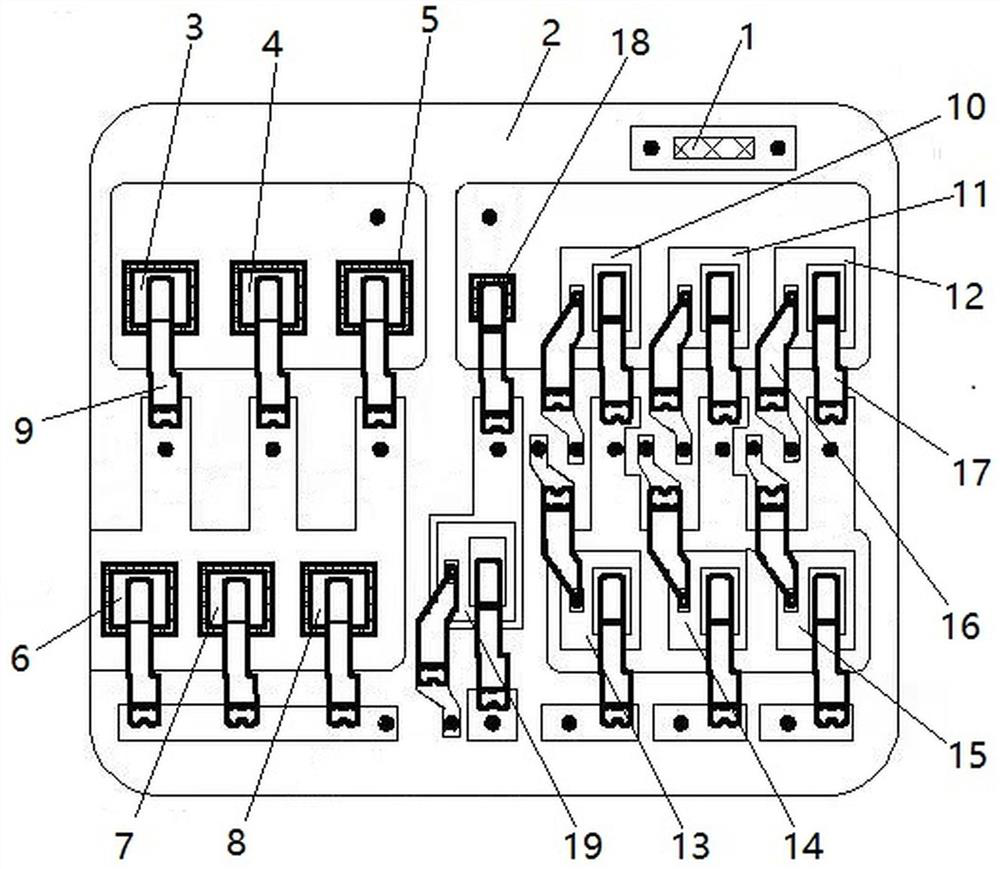
[0048] This embodiment discloses a PIM device, as a basic implementation of the technical solution, including a copper-clad ceramic substrate, a three-phase rectification unit, a three-phase inverter unit, a braking unit and a temperature control detection NTC device 1 .

[0049] The three-phase rectifier unit includes six diode chips arranged on a copper-clad ceramic substrate and clip copper sheets 9 corresponding to the six diode chips, and the six diode chips are diode chip I3, diode chip II4, and diode chip III5. , diode chip Ⅳ6, diode chip Ⅴ7 and diode chip Ⅵ8; six cathodes are connected on the copper-clad ceramic substrate, and the cathodes of diode chip Ⅰ3, diode chip Ⅱ4 and diode chip Ⅲ5 are connected through the copper-clad ceramic substrate; six clip copper sheets 9 One end of each is fixedly connected to the positive poles of the six diode chips, and the other ends of the six clip copper sheets 9 are respectively fixedly connected to the copper-clad ceramic substrat...

Embodiment 2

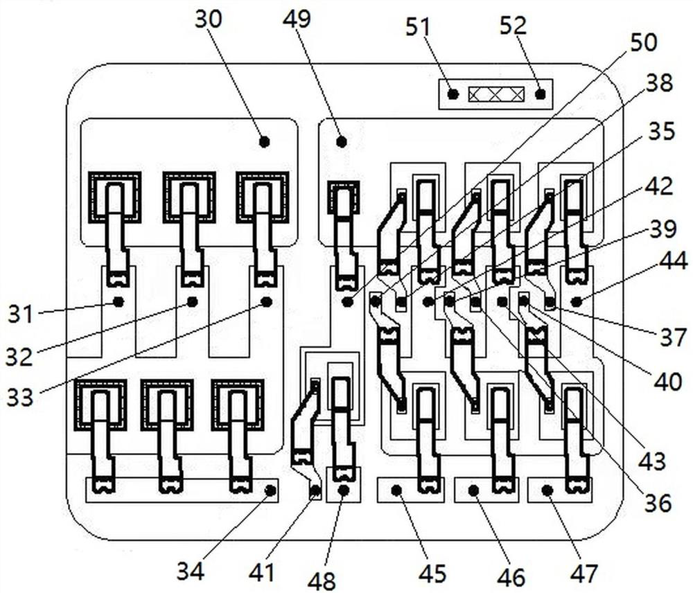
[0054] This embodiment discloses a PIM device, as a preferred implementation of this technical solution, that is, in embodiment 1, the copper-clad ceramic substrate includes a substrate body 2 and is used to connect the three-phase rectifier unit, three-phase inverter The unit, the brake unit and the copper plate unit of the temperature control detection NTC device 1, the copper plate unit is pasted and fixed on the substrate body 2. Specifically, the copper plate unit includes a rectification part and a braking inverter part, wherein the rectification part includes a copper plate I20, a copper plate II21 for arranging a diode chip I3, a diode chip II4 and a diode chip III5, and a copper plate II21 for arranging For the arrangement of diode chip IV6, diode chip V7 and diode chip VI8 copper plate III22; clip copper plate 9 on the positive electrode of diode chip IV6, diode chip IV6, diode chip V7 and diode chip VI8, diode chip I3, diode chip II4 and diode chip III5 The negative...

Embodiment 3

[0056] This embodiment discloses a PIM device, as a preferred implementation of this technical solution, that is, in embodiment 1, IGBT chip I10, IGBT chip II11, IGBT chip III12, IGBT chip IV13, IGBT chip V14 and IGBT chip VI15 Both are composed of IGBT body and freewheeling diode. The three-phase inverter unit of this technical solution adopts an IGBT chip connected in parallel with a freewheeling diode. The IGBT chip will not break down due to the high voltage generated by sudden shutdown, so that the three-phase inverter unit will appear voltage or current in the circuit. It has a protective function when there is a sudden change, and further improves the safety performance of the PIM device.

[0057] Further, all diode chips and IGBT chips are fixed on the copper plate unit by solder paste; all clip copper sheets 9, clip emitter copper sheets 16 and clip control electrode copper sheets 17 are fixed to the copper plate unit by solder paste connection, all clip copper sheet...


PUM


Abstract

The invention relates to the technical field of semiconductor devices, in particular to a PIM device and a manufacturing method thereof, including a copper-clad ceramic substrate and a three-phase rectifier unit, a three-phase inverter unit, a braking unit and a temperature control unit arranged on the copper-clad ceramic substrate. Detect NTC devices; the three-phase rectification unit includes six diode chips arranged on the copper-clad ceramic substrate and the clip copper sheets corresponding to the six diode chips; the three-phase inverter unit includes six IGBT chips, six and six One IGBT chip one-to-one corresponding clip emitter copper sheet and six clip control electrode copper sheets corresponding to six IGBT chips one-to-one; braking unit includes diode chip VII, IGBT chip VII, clip copper sheet, clip emitter copper sheet sheet and clip control pole copper sheet. The PIM device of this technical solution has a compact structure and is easy to use. Applying the PIM device to related circuits can simplify the circuit structure. Based on the clip technology adopted by the PIM device, the performance of the PIM device is stable, which further makes the circuit using the PIM device safe and reliable. .

Description

technical field [0001] The invention relates to the technical field of semiconductor devices, in particular to a PIM device and a manufacturing method thereof. Background technique [0002] PIM circuit is a functional circuit that integrates rectifier circuit, inverter circuit, brake circuit and temperature control switch. ) connected, the circuit is large in size and complex in structure, prone to failure and difficult to maintain. Therefore, the IGBT power integrated module PIM (PowerIntergrated Mondule) has gradually replaced the traditional PIM circuit. The distributed inductance, and the PIM module simplifies the installation process and facilitates maintenance. At present, 25A / 40A / 50A / 75A PIM modules are mostly used in the market for low-power frequency conversion lines below 15kW, which are mainly used in frequency converters, servo motors, frequency conversion household appliances, medical systems and other fields. With the rapid development of the frequency conver...

Claims


Application Information

Patent Timeline
Patent Type & Authority Patents(China)
IPC IPC(8): H02M1/00H01L23/498H02M7/00H02P25/16H02P27/06
CPCH02M1/00H01L23/49811H01L23/49894H01L23/49838H01L23/49844H02M7/003H02P25/16H02P27/06H01L2224/40
Inventor 邓华鲜
Owner 乐山希尔电子股份有限公司
Why Eureka
Try Eureka