Broadband-adjustable non-reflection wave-absorbing device and wave-absorbing method

A broadband, absorbing technology, applied in the optical and microwave fields, can solve the problems of narrow absorbing frequency band, short working bandwidth, and inability to adjust, and achieve the effect of wide absorbing frequency band and long working bandwidth

Pending Publication Date: 2021-10-26
SOUTH UNIVERSITY OF SCIENCE AND TECHNOLOGY OF CHINA
View PDF0 Cites 0 Cited by
  • Summary
  • Abstract
  • Description
  • Claims
  • Application Information

AI Technical Summary

Problems solved by technology

[0005] The technical problem to be solved by the present invention is to provide a broadband adjustable non-reflection absorbing device and a absorbing method for the above-mentioned defects of the prior art, aiming at solving the problem of narrow absorbing frequency band and short working bandwidth of traditional electromagnetic absorbing devices. and can not adjust the problem

Method used


Image

  • Broadband-adjustable non-reflection wave-absorbing device and wave-absorbing method
  • Broadband-adjustable non-reflection wave-absorbing device and wave-absorbing method
  • Broadband-adjustable non-reflection wave-absorbing device and wave-absorbing method

Examples


Embodiment Construction

[0038] In order to make the object, technical solution and advantages of the present invention more clear and definite, the present invention will be further described in detail below with reference to the accompanying drawings and examples. It should be understood that the specific embodiments described here are only used to explain the present invention, not to limit the present invention.

[0039] It should be noted that if there is a directional indication (such as up, down, left, right, front, back...) in the embodiment of the present invention, the directional indication is only used to explain the position in a certain posture (as shown in the accompanying drawing). If the specific posture changes, the directional indication will also change accordingly.

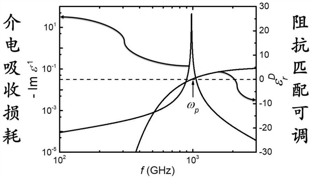
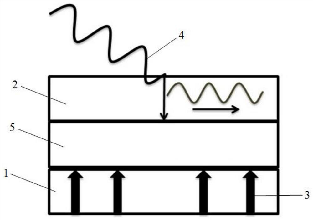
[0040] Electromagnetic wave absorbing devices mainly realize electromagnetic wave absorption in two ways: "internal" and "external". The "external" way is to use a special shape to refract incident electromagnetic wav...


PUM

PropertyMeasurementUnit
Mobilityaaaaaaaaaa

Abstract

The invention discloses a broadband-adjustable non-reflection wave-absorbing device and a wave-absorbing method. The broadband-adjustable non-reflection wave-absorbing device comprises a pumping layer and a wave-absorbing layer arranged on the pumping layer, and the wave-absorbing layer comprises a wave-absorbing material; the pumping layer is used for generating pumping laser; the wave-absorbing layer is used for receiving the pumping laser, inducing free carriers in the wave-absorbing material through the pumping laser, and changing the relative dielectric constant of the wave-absorbing material through the free carriers, so that the wave-absorbing material meets a preset impedance matching condition; and the wave absorbing layer is also used for receiving incident electromagnetic waves and absorbing the incident electromagnetic waves when the wave absorbing material meets a preset impedance matching condition. According to the wave-absorbing device, the free carriers are induced in the wave-absorbing material through the pumping laser, the relative dielectric constant of the wave-absorbing material is changed through the free carriers, the electromagnetic wave-absorbing function of the wave-absorbing device is achieved, the light intensity of the pumping light can be adjusted according to the frequency of incident electromagnetic waves, the working frequency can be adjusted from microwaves to far infrared rays. And the wave-absorbing frequency band is wide and the working bandwidth is long.

Description

technical field [0001] The invention relates to the fields of optics and microwave technology, in particular to a broadband adjustable non-reflection wave-absorbing device and a wave-absorbing method. Background technique [0002] With the extensive use of electronic devices, electromagnetic interference has become a potential hazard that threatens human health and affects the normal operation of electronic devices. Electromagnetic absorbing devices can not only be used for the safety protection of biological health, but also for electromagnetic shielding of electronic devices. [0003] Traditional electromagnetic absorbing devices usually use ferrite-based magnetic absorbing materials and carbon-based dielectric loss absorbing materials as electromagnetic absorbing materials, and through chemical doping or changing the particle size, the electromagnetic The absorbing material achieves impedance matching in the low frequency band. This method makes the absorbing frequency ba...

Claims


Application Information

Patent Timeline
IPC IPC(8): H05K9/00
CPCH05K9/00
Inventor 顾川川项晓东张鹏
Owner SOUTH UNIVERSITY OF SCIENCE AND TECHNOLOGY OF CHINA
Why Eureka
Try Eureka