A kind of semiconductor structure and preparation method thereof

A semiconductor and etching gas technology, which is used in semiconductor/solid-state device manufacturing, semiconductor devices, semiconductor lasers, etc., and can solve problems such as poor growth quality of high-strain semiconductor materials

Active Publication Date: 2021-12-21
GUSU LAB OF MATERIALS +1
View PDF5 Cites 0 Cited by
  • Summary
  • Abstract
  • Description
  • Claims
  • Application Information

AI Technical Summary

Problems solved by technology

[0008] Therefore, the technical problem to be solved by the present invention is to overcome the problem of poor growth quality of high-strain semiconductor materials in the prior art, thereby providing a semiconductor structure and its preparation method

Method used


Image

  • A kind of semiconductor structure and preparation method thereof
  • A kind of semiconductor structure and preparation method thereof
  • A kind of semiconductor structure and preparation method thereof

Examples


preparation example Construction

[0035] An embodiment of the present invention provides a method for preparing a semiconductor structure, please refer to figure 1 , including the following steps:

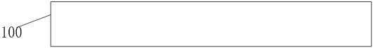
[0036] S1: providing a semiconductor substrate layer;

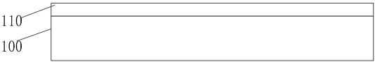
[0037] S2: forming a first strained layer on the semiconductor substrate layer; the step of forming the first strained layer includes: forming a first lattice matching layer on the semiconductor substrate layer, in the first lattice matching layer having at least first atoms and second atoms; etching the first lattice matching layer so that the first lattice matching layer forms a first strained layer, the etching rate of the first atoms is greater than that of the second The etching rate of atoms, the molar ratio of the first atoms and the second atoms in the first strained layer is smaller than the molar ratio of the first atoms and the second atoms in the first lattice matching layer.


PUM

PropertyMeasurementUnit
thicknessaaaaaaaaaa
thicknessaaaaaaaaaa
thicknessaaaaaaaaaa

Abstract

The present invention provides a semiconductor structure and a preparation method thereof. The semiconductor structure includes: providing a semiconductor substrate layer; forming a first strained layer on the semiconductor substrate layer; the step of forming the first strained layer includes: forming the first strained layer on the semiconductor substrate A first lattice matching layer is formed on the bottom layer, and the first lattice matching layer has at least first atoms and second atoms; etching the first lattice matching layer so that the first lattice matching layer forms a first In a strained layer, the etching rate of the first atoms is greater than the etching rate of the second atoms, and the molar ratio of the first atoms and the second atoms in the first strained layer is smaller than the first lattice matching The molar ratio of the first atom to the second atom in the layer. The preparation method of the semiconductor structure makes the quality of the first strain layer better.

Description

technical field [0001] The invention relates to the technical field of semiconductors, in particular to a semiconductor structure and a preparation method thereof. Background technique [0002] Superlattice is a special semiconductor structure widely used in many semiconductor optoelectronic devices, such as semiconductor lasers, photodetectors and avalanche diodes. Among them, the strained superlattice is an important part of the superlattice system. The so-called strained superlattice refers to two materials with a certain degree of lattice mismatch. When using ultra-thin layer epitaxial growth techniques such as molecular beam epitaxy (MBE) and metal organic compound vapor deposition (MOCVD) to prepare heterogeneous structures, rely on The elastic deformation adjusts the interatomic spacing, and finally both achieve a superlattice structure in which the interfacial atomic arrangement still maintains lattice matching. [0003] The emergence of strained superlattice has i...

Claims


Application Information

Patent Timeline
Patent Type & Authority Patents(China)
IPC IPC(8): H01L21/02H01L29/15H01S5/343
CPCH01L21/02392H01L21/02463H01L21/02507H01L21/02546H01L21/0262H01L29/15H01S5/34313
Inventor 程洋万中军王俊庞磊周大勇郭银涛
Owner GUSU LAB OF MATERIALS
Why Eureka
Try Eureka