A semiconductor packaging mold

A semiconductor and mold technology, applied in the field of semiconductor packaging molds, can solve the problems of inconvenient use, reduced packaging efficiency, labor-intensive, etc., and achieve the effect of being easy to use and improving packaging efficiency

Active Publication Date: 2021-12-10
南通迅腾精密设备有限公司
View PDF3 Cites 0 Cited by
  • Summary
  • Abstract
  • Description
  • Claims
  • Application Information

AI Technical Summary

Problems solved by technology

[0005] The object of the present invention is to provide a semiconductor packaging mold, which works by using this device, so as to solve the problem of packaging semiconductors in the above background, usually stacking semiconductors in a packaging box, and then fixing the packaging box cover on the package. On the box, by setting screws on the four corners of the package box cover, a stable package of the semiconductor can be achieved, but this packaging method requires the operator to screw and fix the screws on the four corners of the package box cover one by one, not only need to use a screwdriver, but also It also consumes manpower, greatly reduces the packaging efficiency, and is not easy to use

Method used


Image

  • A semiconductor packaging mold
  • A semiconductor packaging mold
  • A semiconductor packaging mold

Examples


Embodiment Construction

[0037] The following will clearly and completely describe the technical solutions in the embodiments of the present invention with reference to the accompanying drawings in the embodiments of the present invention. Obviously, the described embodiments are only some, not all, embodiments of the present invention. Based on the embodiments of the present invention, all other embodiments obtained by persons of ordinary skill in the art without making creative efforts belong to the protection scope of the present invention.

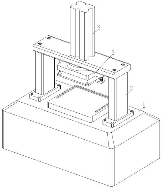
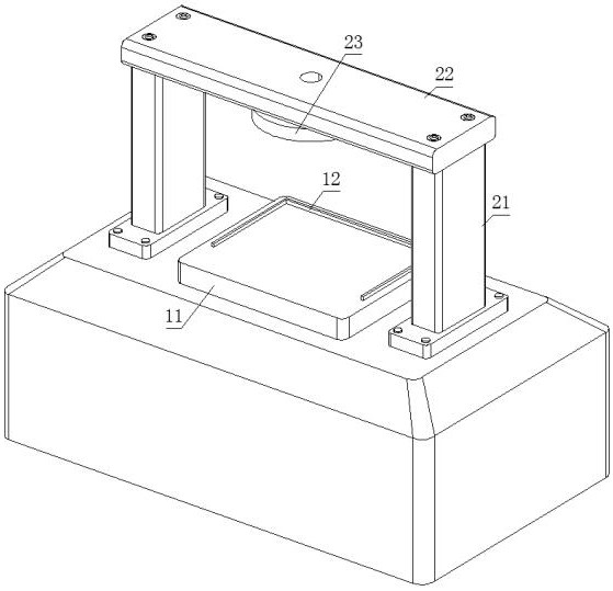
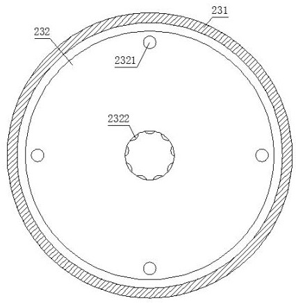
[0038] see figure 1 , figure 2 , Figure 4 and Figure 5 , a semiconductor packaging mold, comprising a mounting base 1 and a concave support frame 2 fixedly installed on the top surface of the mounting base 1, a driving assembly 3 is fixedly installed on the top surface of the middle part of the concave support frame 2, and the output end of the driving assembly 3 is fixed A screw screw assembly 4 is installed, and the screw screw assembly 4 is arranged a...


PUM


Abstract

The invention discloses a semiconductor packaging mold, which relates to the technical field of semiconductors, and comprises a mounting base and a concave support frame fixedly installed on the top surface of the mounting base. A driving component is fixedly installed on the top surface of the middle part of the concave support frame, and the output of the driving component is The screw screw assembly is fixedly installed at the end, and the screw screw assembly is arranged at the lower end of the middle part of the concave support frame. When the operator needs to package the packaging box containing the semiconductor, first place the packaging box in the concave bar, then By placing the screw in the circular placement hole, the electric cylinder is started at this time, and the screw head drives the screw to rotate for packaging work. This setting can not only quickly screw and tighten multiple screws, but also improves the packaging efficiency. At the same time, it cleverly uses the downward displacement of the output end of the electric cylinder, which is easy to use.

Description

technical field [0001] The invention relates to the technical field of semiconductors, in particular to a semiconductor packaging mold. Background technique [0002] Semiconductor refers to a material whose conductivity is between that of a conductor and an insulator at room temperature. Semiconductors are widely used in radios, televisions and temperature measurement. For example, diodes are devices made of semiconductors. Control, ranging from materials between insulators to conductors, whether from the perspective of technology or economic development, the importance of semiconductors is huge, most of today's electronic products, such as computers, mobile phones or digital The core units in the tape recorder are closely related to semiconductors. Common semiconductor materials include silicon, germanium, arsenide, etc., and among various semiconductor materials, silicon is the most influential in commercial applications. When the semiconductor is produced and leaves the ...

Claims


Application Information

Patent Timeline
Patent Type & Authority Patents(China)
IPC IPC(8): H01L21/56
CPCH01L21/565
Inventor 秦小军
Owner 南通迅腾精密设备有限公司
Why Eureka
Try Eureka