Manufacturing method of microchip array optical assembly with ultraviolet light-transmitting substrate and microchip array optical assembly with ultraviolet light-transmitting substrate

A technology of optical components and light-transmitting substrates, applied in optics, nonlinear optics, electrical components, etc., can solve problems such as difficult positioning, welding, and welding area reduction, so as to improve market competitiveness, avoid optical interference, and improve performance effect

Pending Publication Date: 2021-11-09
SUNRICH SEMICON CO LTD
View PDF0 Cites 0 Cited by
  • Summary
  • Abstract
  • Description
  • Claims
  • Application Information

AI Technical Summary

Problems solved by technology

[0007] However, if Figure 9 As shown, in order to install as many mini LED chips 90 as possible on the array substrate 9 with a limited area to improve the picture resolution, the width of each grid 92 is generally about 110-160 μm, which is only smaller than the width of the mini LED chips 90. Slightly larger, it is difficult to accurately position when transferring a huge amount of chips 90 to such a dense grid 92 at the same time, and it is easy to cause some chips 90 to be skewed, resulting in a smaller soldering area between the chips 90 and the driving circuit (not shown in the figure) and making the circuit The impedance of the connection connection increases, and the reduction of the luminance of the chip 90 leads to the problem of uneven brightness
[0008] As the size of the chip gradually shrinks, the picture resolution can undoubtedly be further improved, but in the assembly process, precise positioning has also become a more difficult problem: especially how to accurately form the grid-shaped fence 94 that shields the side light, if you want to move it first Turn the chip and weld it to the drive circuit. When the microchip is installed deflected or even partially occupies the position that should be spaced, it is difficult to form the grid-shaped fence accurately; There is still a certain height in itself, and the microchip cannot be correctly placed on the drive circuit for soldering

Method used


Image

  • Manufacturing method of microchip array optical assembly with ultraviolet light-transmitting substrate and microchip array optical assembly with ultraviolet light-transmitting substrate
  • Manufacturing method of microchip array optical assembly with ultraviolet light-transmitting substrate and microchip array optical assembly with ultraviolet light-transmitting substrate
  • Manufacturing method of microchip array optical assembly with ultraviolet light-transmitting substrate and microchip array optical assembly with ultraviolet light-transmitting substrate

Examples


Embodiment Construction

[0033] The present invention will be further elaborated below in conjunction with the accompanying drawings and specific embodiments. These examples should be understood as only for illustrating the present invention but not for limiting the protection scope of the present invention. After reading the contents of the present invention, those skilled in the art can make various changes or modifications to the present invention, and these equivalent changes and modifications also fall within the scope defined by the claims of the present invention.

[0034] first preferred embodiment

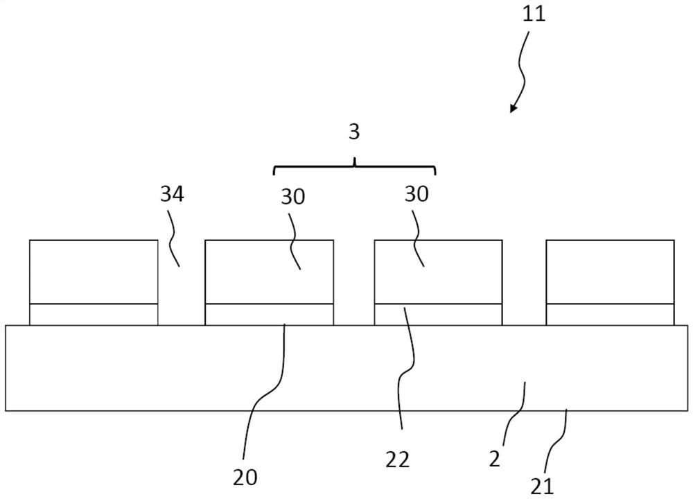
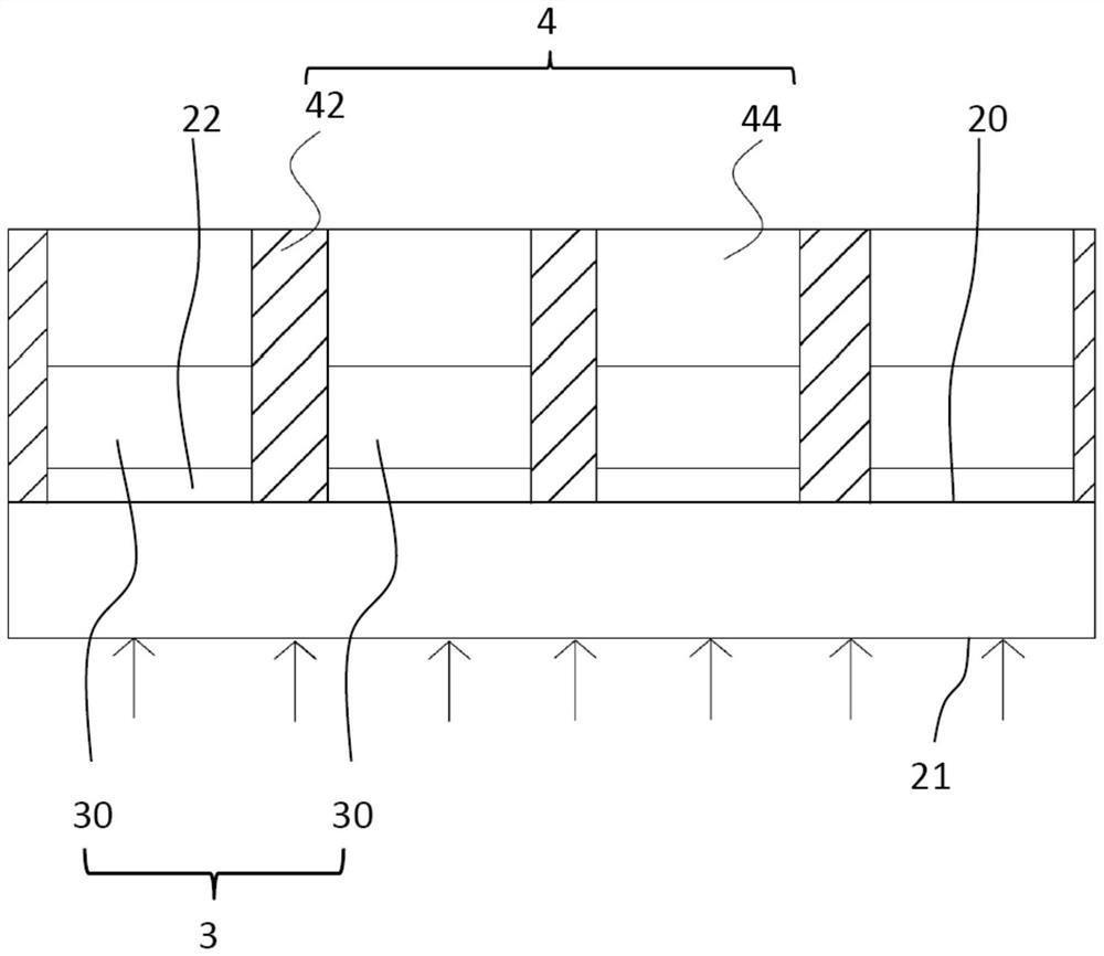
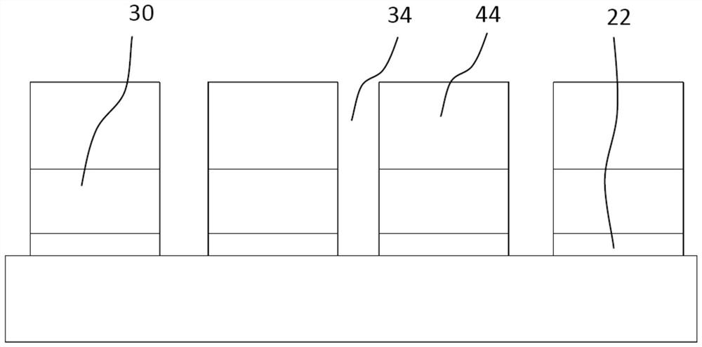
[0035] The first preferred embodiment of the present invention provides a microchip array optical assembly with an ultraviolet light-transmitting substrate, taking a backlight module for a liquid crystal display as an example, first as figure 1 As shown, a piece of alkali-free glass sheet with a transmittance of more than 80% for ultraviolet light, full-band visible light, and infrared light at ...


PUM


Abstract

The invention discloses a microchip array optical assembly with an ultraviolet light-transmitting substrate, which comprises an ultraviolet light-transmitting array substrate, a microchip array, a shading part and a transparent protection unit, wherein the ultraviolet light-transmitting array substrate is provided with a light-transmitting substrate body and a group of driving circuit units, the light-transmitting substrate body is used for allowing part of ultraviolet excitation light with specific wavelength to penetrate through, and is provided with a setting surface for setting the driving circuit units and a bottom surface opposite to the setting surface; the microchip array can block the ultraviolet exciting light and comprises a plurality of microchips which are arranged at intervals by a gap and are respectively driven by the driving circuit units, each microchip is used for emitting and / or receiving at least one piece of light, and each microchip can block the penetration of the ultraviolet exciting light; the shading part is filled in the gap; and the transparent protection unit covers the microchip array and the driving circuit units and is used for sealing the microchip array on the ultraviolet-transmitting array substrate in an airtight manner. In addition, the invention further discloses a manufacturing method of the microchip array optical assembly with the ultraviolet light transmitting substrate.

Description

technical field [0001] The invention relates to a microchip array optical assembly, in particular to a microchip array optical assembly with an ultraviolet light-transmitting substrate. Background technique [0002] Light-emitting diodes (LEDs, light-emitting diodes) replaced traditional small tungsten bulbs when they were invented, and were used as indicator lights on various devices. Later, with the continuous improvement of phosphor materials and packaging technology, LEDs gradually moved towards It is large-scale, high-lumen and has power-saving characteristics, so it replaces the old cold-cathode tube and is used in the backlight module of the liquid crystal display as a light source that is passively turned on and off, mainly imitating the cold-cathode tube in the form of a light bar. It is configured according to the configuration method in the backlight module. [0003] Later, due to people's increasing requirements for the native contrast and picture response speed...

Claims


Application Information

Patent Timeline
IPC IPC(8): H01L27/15H01L33/48H01L33/56H01L33/62G02F1/133G02F1/13357
CPCH01L27/156H01L33/56H01L33/48H01L33/62G02F1/13306H01L2933/0066H01L2933/0033H01L2933/005
Inventor 曾国书邱昱维庄弘毅
Owner SUNRICH SEMICON CO LTD
Why Eureka
Try Eureka