
Circuit board, preparation method thereof and backlight board

A technology for circuit boards and conductive circuit layers, applied in the field of backlight boards, can solve problems such as product quality problems, copper circuits are prone to peeling, and the bonding force between substrates and copper circuits is reduced, and the effect of high light reflectivity is achieved.

Pending Publication Date: 2021-11-09
AVARY HLDG (SHENZHEN) CO LTD +1
View PDF4 Cites 0 Cited by
  • Summary
  • Abstract
  • Description
  • Claims
  • Application Information

AI Technical Summary

Problems solved by technology

[0004] However, the titanium dioxide powder in the substrate will reduce the bonding force between the substrate and the copper circuit, and as the addition of titanium dioxide powder increases, the bonding force between the substrate and the copper circuit will even drop to 0.5kgf / cm Below, which makes the copper lines easy to peel off, resulting in product quality problems

Method used


Image

  • Circuit board, preparation method thereof and backlight board
  • Circuit board, preparation method thereof and backlight board
  • Circuit board, preparation method thereof and backlight board

Examples


Embodiment Construction

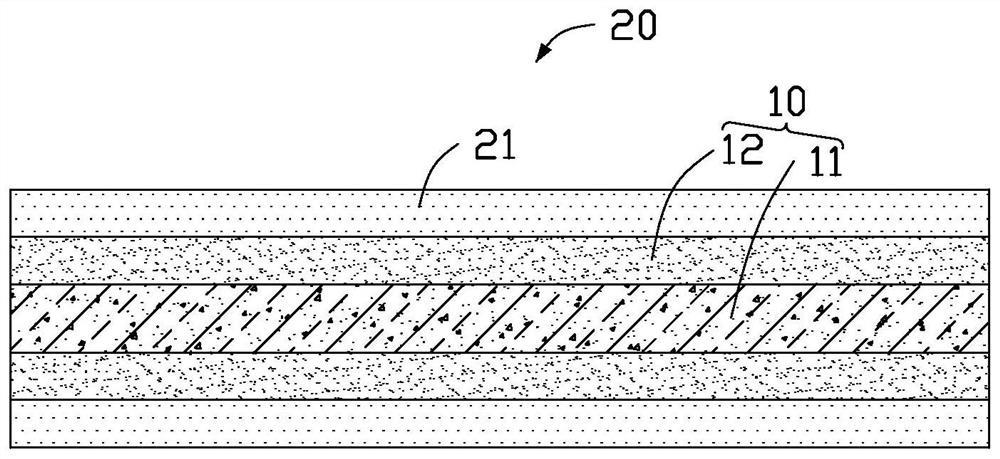
[0038] see Figure 1 to Figure 6 A preferred embodiment of the present application provides a method for preparing a circuit board 100. According to different requirements, the order of steps in the method can be changed, and some steps can be omitted or combined. Described preparation method comprises the steps:

[0039] Step one, see figure 1 , provide glass fiber cloth 11.

[0040] Step two, see figure 2 , the glass fiber cloth 11 is impregnated in the first adhesive, and the bonding sheet 10 is obtained after curing.

[0041] Wherein, the first adhesive layer 12 is formed after the first adhesive is cured, and the first adhesive layer 12 is filled in the gap of the glass fiber cloth 11, and is also formed on two opposite sides of the glass fiber cloth 11. On the surface. In this embodiment, the glass fiber cloth 11 impregnated with the first adhesive may be baked by a gluing machine to cure the first adhesive.

[0042] In this embodiment, the first adhesive is a whi...


PUM

PropertyMeasurementUnit
thicknessaaaaaaaaaa
thicknessaaaaaaaaaa
reflectanceaaaaaaaaaa

Abstract

The invention discloses a preparation method of a circuit board, which comprises the steps of providing a glass fabric, impregnating the glass fabric in a first adhesive, and curing to obtain a bonding sheet; coating the surface of the bonding sheet with a second adhesive, wherein the light reflectivity of the second adhesive is less than that of the first adhesive, and a composite base material is obtained after curing; forming a first conductive circuit layer on the surface of the composite base material; and forming a first protection layer on the surface of the first conductive circuit layer, wherein part of the first conductive circuit layer is exposed to the first protection layer to form a first welding pad and a second welding pad. The invention further provides a circuit board and a backlight board. According to the invention, the peeling strength of the conductive circuit layer is not reduced while the light reflectivity is high.

Description

technical field [0001] The present application relates to a printed circuit board technology, in particular to a circuit board, a preparation method of the circuit board and a backlight board having the circuit board. Background technique [0002] Submillimeter light-emitting diode (Mini LED) refers to LEDs with a grain size of about tens of microns. As a new generation of LED display technology, it can be applied to small-pitch LED displays below P1.0 mm. When used as a backlight, Mini LEDs are transferred to rigid or flexible substrates in batches using COB or "four-in-one" technology. By increasing the number of light sources, the light mixing distance (OD distance) is reduced, thereby reducing the thickness of the backlight panel. [0003] Usually, in order to improve luminous efficiency, Mini LED needs to be matched with a white high-reflectivity substrate (the emissivity needs to exceed 80%). In the prior art, the substrate is made of a polymer resin added with a suf...

Claims


Application Information

Patent Timeline
Patent Type & Authority Applications(China)
IPC IPC(8): H05K1/03H05K1/02
CPCH05K1/038H05K1/0274
Inventor 侯宁
Owner AVARY HLDG (SHENZHEN) CO LTD
Learn More