Metalens array device
A lens array and device technology, applied in the field of nano optics, can solve the problems of inability to obtain additional information, large space optical path, single function, etc., and achieve the effect of reducing the space volume of the system
- Summary
- Abstract
- Description
- Claims
- Application Information
AI Technical Summary
Problems solved by technology
Method used
Image

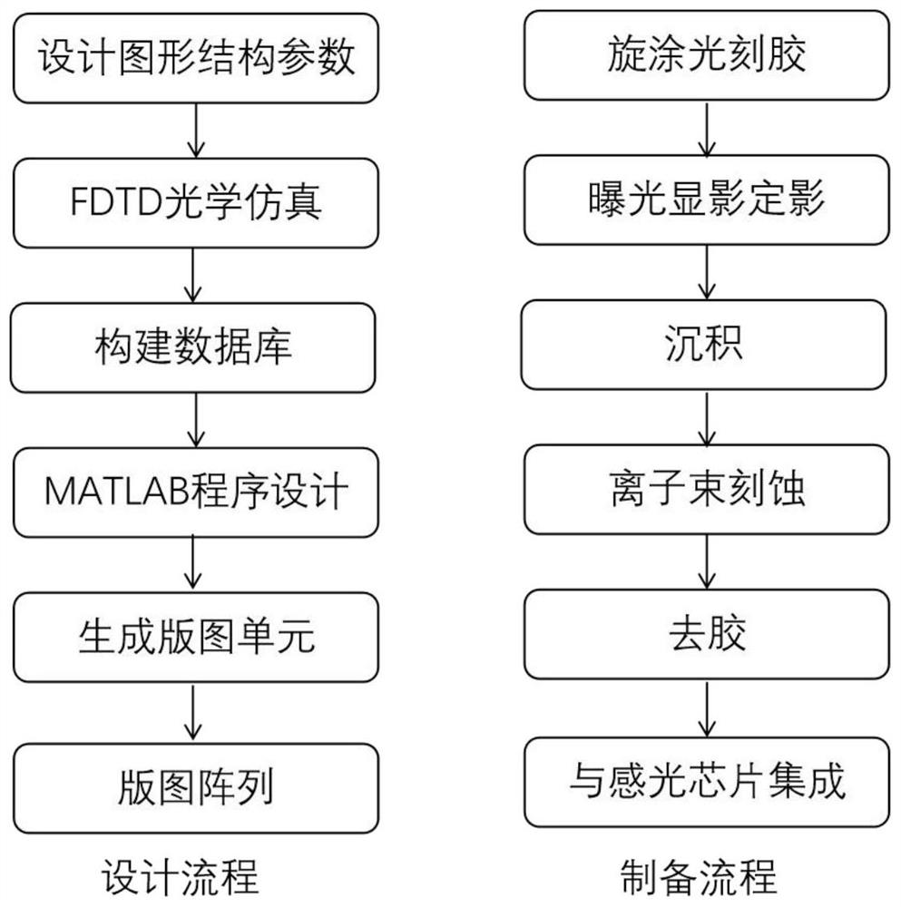
Examples
example 1
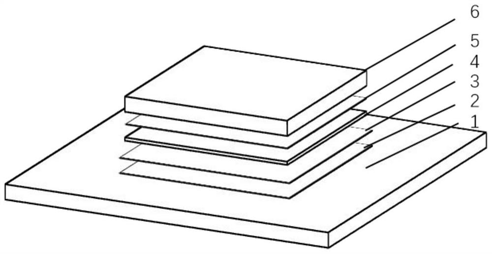
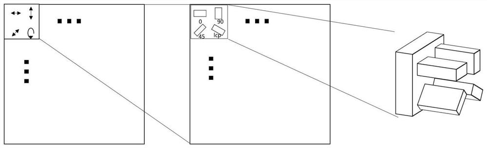
[0044] Example 1 Hardman sensor
[0045] For the polarization detection function, that is to obtain the light intensities of the four polarization components mentioned above, at this time Figure 4 The size of b in is close to f, because the polarization detection is to obtain the four parameters of the polarization stokes, and the expression of the parameters is:
[0046]
[0047] The expression for obtaining light intensity information is:
[0048]
[0049]
[0050]
[0051]
[0052] Among them, I is the light intensity, δ is the phase difference between the two orthogonal directions of light, the polarization state can be calculated by simple linear transformation, and the distribution of several common polarized light can be obtained according to the distribution of the focal spot of the lens out, such as Figure 5 shown. This is because the four focal points of the metalens are sensitive to four kinds of polarized light respectively. From left to right a...
example 2
[0053] Example 2 Polarized Light Field Camera
[0054] Figure 4 The focal length f in is close to the distance between the two, and the specific distance depends on the designed image size. The size of the image depends on the object distance a and the image distance b, and the imaging formula is:
[0055]
[0056] Among them, a is the distance from a certain image surface of the main lens to the lens array. Different a represents different depths, and the final image sizes are also different. Therefore, by selecting sub-image blocks of different sizes on the CMOS photosensitive chip, you can Select the imaging of objects at different depths. In order to obtain light field information and non-overlap between sub-images, it is also necessary to ensure that the image is reduced by more than two times, that is, a is greater than twice b. For the common Kepler and Galileo imaging modes, the relationship between f and b can be obtained ,
[0057] f / 2
[005...
PUM
| Property | Measurement | Unit |
|---|---|---|
| Thickness | aaaaa | aaaaa |
| Thickness | aaaaa | aaaaa |
| Height range | aaaaa | aaaaa |
Abstract
Description
Claims
Application Information
 - R&D Engineer
- R&D Manager
- IP Professional
- Industry Leading Data Capabilities
- Powerful AI technology
- Patent DNA Extraction
Browse by: Latest US Patents, China's latest patents, Technical Efficacy Thesaurus, Application Domain, Technology Topic.
© 2024 PatSnap. All rights reserved.Legal|Privacy policy|Modern Slavery Act Transparency Statement|Sitemap