
Method for rounding top corner of groove and semiconductor structure

A semiconductor and trench technology, applied in semiconductor devices, semiconductor/solid-state device manufacturing, electrical components, etc., can solve problems such as adverse effects of semiconductor device performance, semiconductor device defects, high production costs, etc., to achieve easier control of the etching process, Excellent sharp corners, the effect of reducing production costs

Pending Publication Date: 2021-11-26
SIEN QINGDAO INTEGRATED CIRCUITS CO LTD
View PDF7 Cites 1 Cited by
  • Summary
  • Abstract
  • Description
  • Claims
  • Application Information

AI Technical Summary

Problems solved by technology

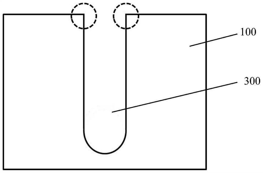
However, after the etching of the common trench structure is completed, the angle between the top and the substrate surface is about 90 degrees, such as figure 1 As shown in , the formed sharp corners are very likely to cause leakage, which can easily have a negative impact on the performance of semiconductor devices. Therefore, it is usually necessary to round the sharp corners to make the top of the trench form a smooth corner
[0003] In the prior art, the rounding of sharp corners is usually performed by thermal oxidation after trench etching or additional high-density plasma (HDP) etching to obtain a trench with a slope at the top, but these methods not only The process is complex and difficult, the production cost is expensive, and because high-density plasma etching will introduce some impurity pollution at the same time, it is easy to bring defects to semiconductor devices

Method used


Image

  • Method for rounding top corner of groove and semiconductor structure
  • Method for rounding top corner of groove and semiconductor structure
  • Method for rounding top corner of groove and semiconductor structure

Examples


Embodiment Construction

[0047] The embodiments of the present invention will be described below by specific embodiments, and those skilled in this specification can easily understand other advantages and efficacy of the present invention. The present invention can also be implemented or applied by different embodiments, and various details in this specification may also perform various modifications or changes without departing from the spirit of the present invention. It should be noted that the features in the following examples and embodiments may be combined with each other in the case of unlilled.

[0048] Inspections, the illustrations provided in the embodiments of the present invention will illustrate the basic consequences of the present invention in a schematic manner, which exhibits only the components associated with the components associated with the present invention in the figure, not in accordance with the number of components, shape and size. The morphology, quantity and proportion of ea...


PUM


Abstract

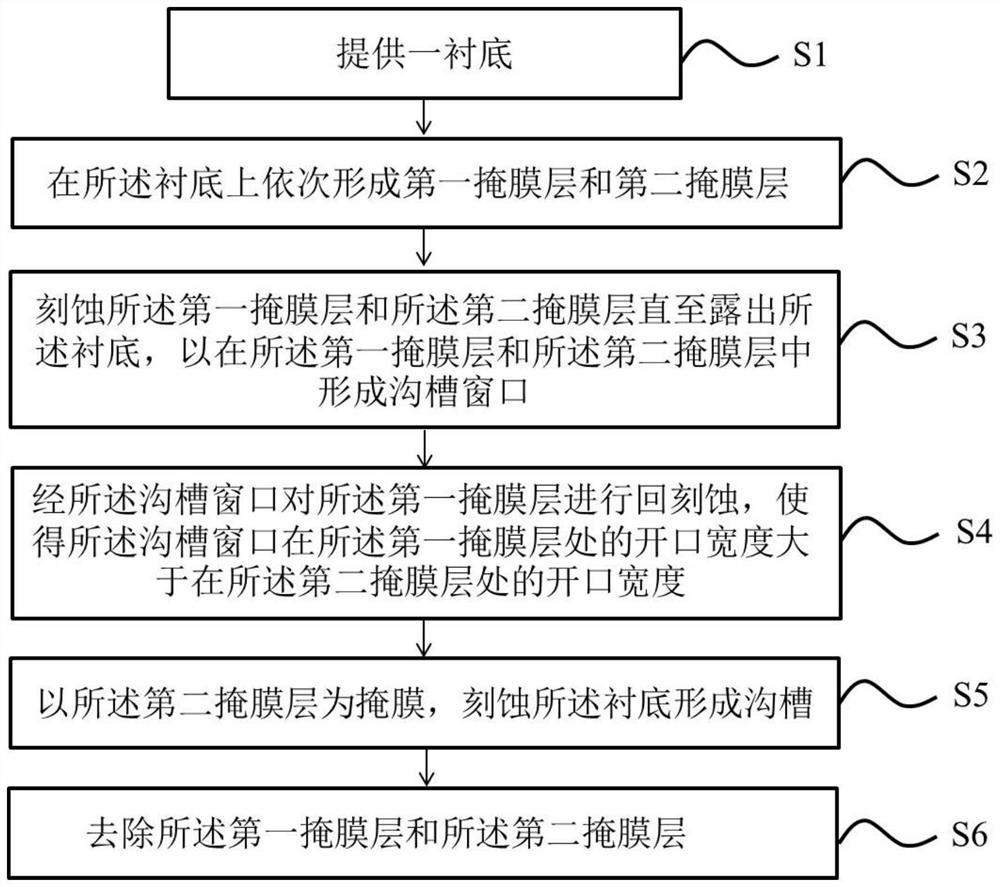
The invention provides a method for rounding a top corner of a groove and a semiconductor structure. According to the method, the top corner of the groove is made to be always in an exposed state in a groove forming process through the back etching of a first mask layer next to a substrate, and the top sharp corner of the groove can be synchronously rounded in a groove etching process, so that the smooth and round top corner of the groove can be formed. With the method adopted, a sharp corner at the top of the groove is eliminated, the smooth and round top corner of the groove can be formed while the groove is etched, no independent rounding operation needs to be added, the whole method is simple in process, and the production cost is greatly reduced; and the first mask layer is subjected to back etching by adopting wet etching, so that the whole etching process is easier to control, the back etching amount can be more accurately controlled, and the subsequent rounding of the top corner of the groove is simpler and easier to control. According to the semiconductor structure with the groove top corner formed by the method, the electric leakage phenomenon can be effectively avoided, the breakdown voltage can be improved, and the reliability of the semiconductor structure can be ensured.

Description

Technical field [0001] The present invention relates to the field of semiconductor technology, and more particularly to a circulation method and a semiconductor structure of a trench angle. Background technique [0002] During the manufacturing process of the semiconductor device, in many cases, it is necessary to etch the groove structure, such as the gate structure in the trench structure power device, is filled with polysilicon into the groove structure, and then the ditch formed by the STI process The groove isolation structure is to fill the insulating material to the groove structure. However, the normal trench structure etching is completed at the top of the surface of the substrate 90 degrees, such as figure 1 As shown in the above, the sharp angle formed is easy to generate leakage, and it is easy to adversely affect the performance of the semiconductor device, so it is typically a rounding process to the trench to form a sleek corner of the trench. [0003] In the prior...

Claims


Application Information

Patent Timeline
Patent Type & Authority Applications(China)
IPC IPC(8): H01L21/308H01L21/762H01L21/28H01L29/06H01L29/423
CPCH01L21/76224H01L21/3081H01L21/3086H01L29/401H01L29/0649H01L29/0607H01L29/4236
Inventor 徐若男赵月梅冯志明曾伟雄
Owner SIEN QINGDAO INTEGRATED CIRCUITS CO LTD
Learn More