
Manufacturing method of high-voltage thick gate oxide

A manufacturing method and thick gate oxide technology, which are applied in semiconductor/solid state device manufacturing, semiconductor devices, electrical components, etc., can solve the problems affecting the reliability of thick gate oxide related device performance, poor reliability of thermal oxide growth, and thin gate oxide. and other problems, to achieve the effect of improving reliability and performance of high-voltage devices, low cost, and eliminating sharp corners.

Active Publication Date: 2021-04-09
HUA HONG SEMICON WUXI LTD
View PDF4 Cites 0 Cited by
  • Summary
  • Abstract
  • Description
  • Claims
  • Application Information

AI Technical Summary

Problems solved by technology

Due to the inherent structural characteristics of STI, when making high-voltage devices and growing thick gate oxides, there will always be problems with thinner gate oxides and sharp corners at the corners of STI, which directly affects the reliability and related issues of thick gate oxides. Device performance
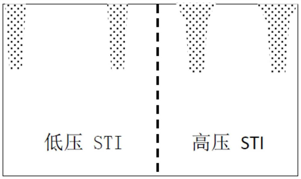
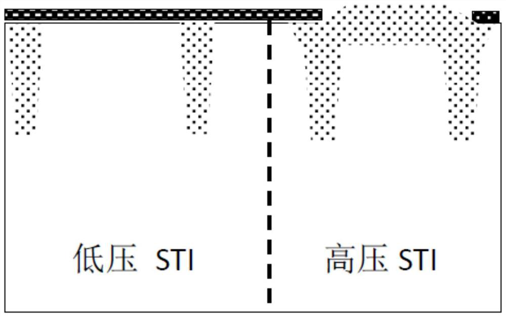
[0003] At present, there are some STI thick gate oxide generation solutions to solve the STI corner problem. One is to use a double STI process, such as figure 1 , figure 2 As shown, it is necessary to add a plate to do the high-voltage STI process alone, and the cost is relatively high; the other is to use the oxide layer (oxide) deposition process, such as image 3 As shown, this can only be partially improved, and its reliability is worse than that of thermal oxygen growth

Method used


Image

  • Manufacturing method of high-voltage thick gate oxide
  • Manufacturing method of high-voltage thick gate oxide
  • Manufacturing method of high-voltage thick gate oxide

Examples


Embodiment 1

[0040] The manufacturing method of high-voltage thick gate oxide includes the following steps:

[0041] 1. Deposit a pad layer silicon oxide (PAD Oxide) 11 on the silicon substrate 1, and deposit a pad layer silicon nitride (PAD SIN) 21 on the pad layer silicon oxide 11; perform shallow trench isolation (STI) photolithography and etching ; Perform shallow trench isolation (STI) silicon oxide filling and chemical mechanical polishing (Oxide Filling and CMP), such as Figure 4 shown;

[0042] 2. Deposit mask silicon nitride 22 on the silicon wafer, and deposit mask silicon oxide 12 on the mask silicon nitride 22;

[0043] 3. Using the mask silicon oxide 12 as a hard mask, photolithography and etching remove the mask silicon oxide 12 and mask silicon nitride 22 in the high-voltage thick gate oxide region, and retain the two shallow grooves in the high-voltage thick gate oxide region Pad silicon nitride 21 between isolation (STI), such as Figure 8 shown;

[0044] 4. Perform t...

Embodiment 2

[0050] Based on the manufacturing method of high-voltage thick gate oxide in Embodiment 1, after step 5, the pad layer silicon oxide 11 on the silicon substrate 1 between the two shallow trench isolations and the mask silicon nitride outside the high-voltage thick gate oxide region are removed The mask silicon oxide 12 on 22 is cleaned, and then step six is ​​performed;

[0051] In step six, a second thermal oxidation growth is performed on the silicon substrate 1 in the high-voltage thick gate oxide region to generate high-voltage thick gate oxide.

[0052]The manufacturing method of the high-voltage thick gate oxide of the second embodiment is to remove the pad silicon oxide 11 deposited on the silicon substrate 1 between the two shallow trench isolations (STIs), and then place the pad silicon oxide 11 on the silicon substrate 1 The high-voltage thick gate oxide is generated through the second thermal oxidation growth, which can reduce the impurities of the high-voltage thic...

Embodiment 3

[0054] Based on the manufacturing method of high-voltage thick gate oxide in Embodiment 1, wet oxygen oxidation, water vapor oxidation or dry oxygen oxidation is used for the first thermal oxidation growth;

[0055] The second thermal oxidation growth adopts wet oxygen oxidation, water vapor oxidation or dry oxygen oxidation.

[0056] Preferably, dry oxygen oxidation is used for the first thermal oxidation growth, and the passivation effect is good; wet oxygen oxidation or water vapor oxidation is used for the second thermal oxidation growth, and the oxidation speed is fast.

[0057] Preferably, the first thermal oxidation growth uses a wet oxygen oxidation process, the operating temperature of the wet oxygen oxidation process is 800°C to 900°C (for example, 850°C), and the oxygen flow rate is 24 to 26 liters / minute (for example, 25 liters / minute ), the flow rate of hydrogen is 26~28 liters / minute (for example 27 liters / minute). In the wet oxygen oxidation process, oxygen can...


PUM


Abstract

The invention discloses a manufacturing method of a high-voltage thick gate oxide, and the method comprises the following steps of: depositing cushion silicon oxide on a silicon substrate, and depositing cushion silicon nitride on the cushion silicon oxide; carrying out shallow trench isolation photoetching, etching, silicon oxide filling and chemical mechanical grinding; sequentially depositing mask silicon nitride and mask silicon oxide on a silicon wafer; removing the mask silicon oxide and the mask silicon nitride in ae high-voltage thick gate oxide region through photoetching and etching processes, and reserving the cushion silicon nitride between the two shallow trench isolations in the high-voltage thick gate oxide region; carrying out first thermal oxidation growth to passivate the shallow trench isolation corner of the high-voltage gate oxide region; removing the cushion silicon nitride between the two shallow trench isolations of the high-voltage thick gate oxide region; and carrying out second thermal oxidation growth to generate the high-voltage thick gate oxide. The thick gate oxide and the STI corner gate oxide of the high-voltage device manufactured by the manufacturing method of the high-voltage thick gate oxide are thickened, passivated and smooth, the STI sharp corner problem can be eliminated, the reliability of the high-voltage thick gate oxide and the performance of the high-voltage device are improved, the process is simple, and the cost is low.

Description

technical field [0001] The invention relates to semiconductor manufacturing technology, in particular to a method for manufacturing high-voltage thick gate oxide. Background technique [0002] With the shrinking of the process size, the isolation process of semiconductor devices has changed from LOCOS (LOCAL Oxidation Of Silicon, local silicon oxidation isolation) to STI (Shallow Trench Isolation, shallow trench isolation). The process of filling the trench with a dielectric material is formed. Due to the inherent structural characteristics of STI, when making high-voltage devices and growing thick gate oxides, there will always be problems with thinner gate oxides and sharp corners at the corners of STI, which directly affects the reliability and related issues of thick gate oxides. device performance. [0003] At present, there are some STI thick gate oxide generation solutions to solve the STI corner problem. One is to use a double STI process, such as figure 1 , fig...

Claims


Application Information

Patent Timeline
Patent Type & Authority Applications(China)
IPC IPC(8): H01L21/28H01L29/423
CPCH01L29/42364H01L21/28229H01L21/28158H01L21/76235H01L21/02238H01L21/02255H01L21/02164H01L21/0217H01L21/02359H01L21/31144H01L21/76224
Inventor 刘俊文
Owner HUA HONG SEMICON WUXI LTD
Learn More