Eureka AIR delivers breakthrough ideas for toughest innovation challenges, trusted by R&D personnel around the world.

Semiconductor device based on dummy channel and manufacturing method thereof

A manufacturing method and semiconductor technology, applied in the direction of semiconductor devices, semiconductor/solid-state device manufacturing, electrical components, etc., can solve problems such as increasing the risk of device failure, achieve the effects of preventing breakdown, improving conduction current capability, and preventing failure

Active Publication Date: 2022-02-08
BEIJING CENTURY GOLDRAY SEMICON CO LTD
View PDF5 Cites 0 Cited by
  • Summary
  • Abstract
  • Description
  • Claims
  • Application Information

AI Technical Summary

Problems solved by technology

However, in the existing technology, the doping of the JFET region adopts the method of central implantation, which will cause the electric field to further concentrate on the surface of the JFET region, increasing the risk of device failure

Method used


Image

  • Semiconductor device based on dummy channel and manufacturing method thereof
  • Semiconductor device based on dummy channel and manufacturing method thereof
  • Semiconductor device based on dummy channel and manufacturing method thereof

Examples


Embodiment Construction

[0050] The following will clearly and completely describe the technical solutions in the embodiments of the present invention with reference to the accompanying drawings in the embodiments of the present invention. Obviously, the described embodiments are only some, not all, embodiments of the present invention. Based on the embodiments of the present invention, all other embodiments obtained by persons of ordinary skill in the art without making creative efforts belong to the protection scope of the present invention.

[0051] SiC power MOSFET is a unipolar voltage control device, which is mainly used in power supply and power processing system to control the conversion of electric energy. Compared with traditional Si-based power devices, SiC devices are easier to achieve high voltage, low loss and high power density, and thus gradually become the mainstream of the market.

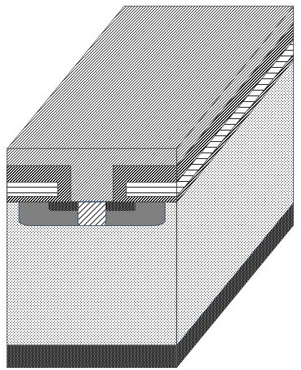
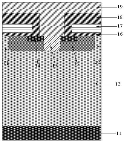
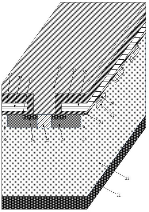
[0052] Such as figure 1 and figure 2 as shown, figure 1 is a schematic diagram of the structure of...


PUM


Abstract

The present application discloses a semiconductor device based on a dummy channel and a manufacturing method thereof. The semiconductor device includes: a semiconductor substrate having opposite first and second surfaces; an epitaxial layer disposed on the first surface; The epitaxial layer is disposed away from the well region, the first JFET region and the second JFET region in the first surface; the well region is disposed away from the source region in the surface of the semiconductor substrate; wherein, the first Both a JFET region and the second JFET region have a plurality of first ion implantation regions; in the same JFET region, a plurality of the first ion implantation regions are arranged sequentially in a first direction; the first directions are parallel on the semiconductor substrate and perpendicular to the wiring direction of the first JFET region and the second JFET region. Applying the technical solution provided by the invention, by sequentially implanting B ions in the JFET region, the electric field on the surface of the JFET can be effectively reduced, device failure can be prevented, and the conduction current capability of the device can be improved at the same time.

Description

technical field [0001] The invention relates to the technical field of semiconductor manufacturing, in particular to a semiconductor device based on a dummy channel and a manufacturing method thereof. Background technique [0002] For a long time, Si materials have occupied a dominant position in the semiconductor field and are used in high-temperature and high-frequency circuits. However, with the advancement of technology and the expansion of application fields, Si-based devices are becoming more and more difficult to meet the requirements of harsher environments and higher performance, so people turn their attention to wide bandgap semiconductors. SiC material is considered to be a very potential third-generation semiconductor material. SiC material has higher breakdown field strength, higher carrier saturation velocity and higher thermal conductivity than Si material, making SiC power electronic devices Compared with similar devices of Si, it has the characteristics of ...

Claims


Application Information

Patent Timeline
Patent Type & Authority Patents(China)
IPC IPC(8): H01L29/78H01L29/06H01L21/04
CPCH01L29/7802H01L29/063H01L29/0619H01L21/0445H01L29/66068
Inventor 孙博韬黎磊徐妙玲张晨邱艳丽王志超冯云艳李天运
Owner BEIJING CENTURY GOLDRAY SEMICON CO LTD
Why Eureka
Eureka Blog
Learn More