
Wave-soldering spot defect detection method and system

A defect detection and solder joint detection technology, which is applied in image data processing, complex mathematical operations, instruments, etc., can solve problems such as unsatisfactory detection accuracy, and achieve the effect of facilitating effective extraction, improving yield rate, and improving accuracy rate

Active Publication Date: 2021-11-30
GUANGDONG UNIV OF TECH
View PDF5 Cites 9 Cited by
  • Summary
  • Abstract
  • Description
  • Claims
  • Application Information

AI Technical Summary

Problems solved by technology

[0005] In order to solve the problem of unsatisfactory detection accuracy of the current wave soldering point defect detection method based on automatic optical detection, the present invention proposes a wave peak soldering point defect detection method and system, improve the accuracy of solder joint defect detection, and optimize the detection effect of solder joint defects

Method used


Image

  • Wave-soldering spot defect detection method and system
  • Wave-soldering spot defect detection method and system
  • Wave-soldering spot defect detection method and system

Examples


Embodiment 1

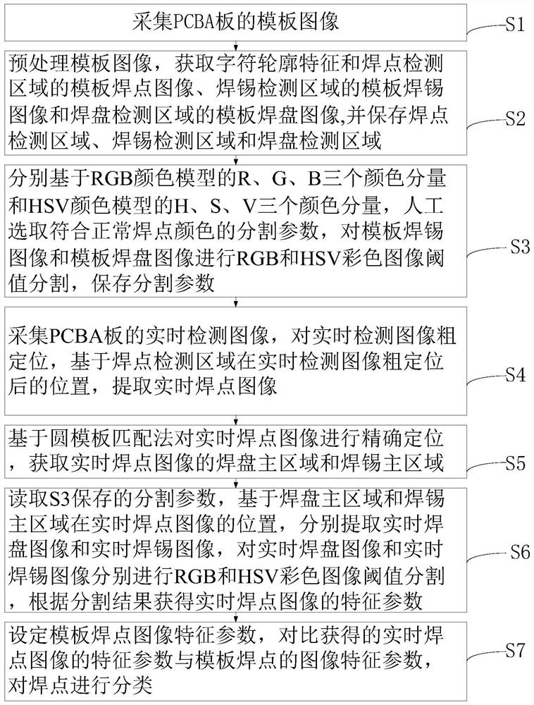
[0092] Such as figure 1 , the application proposes a wave soldering spot detection method, comprising the following steps:

[0093] S1. Collect the template image of the PCBA board;

[0094] S2. Preprocess the template image, obtain the character outline feature and the template solder joint image of the solder joint detection area, the template solder image of the solder detection area and the template pad image of the solder pad detection area, and save the solder joint detection area and the solder detection area and pad detection area;

[0095] S3. Based on the three color components of R, G, and B of the RGB color model and the three color components of H, S, and V of the HSV color model, manually select the segmentation parameters that conform to the normal solder joint color, and compare the stencil solder image and the stencil solder Perform RGB and HSV color image threshold segmentation on the disk image, and save the segmentation parameters;

[0096] S4. Collect t...

Embodiment 2

[0156] see Figure 7 , the application also proposes a wave solder joint detection system, the system is used to implement the wave solder joint detection method described in embodiment 1, the wave solder joint detection system includes:

[0157] Image acquisition module, for collecting the template image of PCBA board;

[0158] The preprocessing module is used to preprocess the template image, obtain the template solder joint image of the character outline feature and the solder joint detection area, the template solder image of the solder detection area and the template pad image of the solder pad detection area, and save the solder joint detection area , solder detection area and pad detection area;

[0159] The first threshold segmentation module is based on the three color components of R, G, and B of the RGB color model and the three color components of H, S, and V of the HSV color model. RGB and HSV color image threshold segmentation for image and stencil pad image, s...


PUM


Abstract

The invention provides a wave-soldering spot defect detection method and a wave-soldering spot defect detection system, which solve the problem of non-ideal detection accuracy of the current wave-soldering spot defect detection method based on automatic optical detection.The method comprises the following steps: firstly, PCBA template image collection, preprocessing and color image threshold segmentation are carried out; then color image threshold segmentation is carried out on a detection area at the same time on the basis of R, G and B color components of the RGB color model and H, S and V color components of the HSV color model, the threshold segmentation process is optimized, effective extraction of a defect area is facilitated, a circular template matching optimization method is designed, positioning of soldering tin and a bonding pad in a wave-soldering spot is optimized; a more accurate defect area is provided for subsequent second threshold segmentation, finally, the obtained welding spot image feature parameters are compared with the original image feature parameters, a defect sample is detected, the accuracy of welding spot defect detection is improved, so that the yield of PCBA boards produced in a factory can be increased.

Description

technical field [0001] The present invention relates to the technical field of machine vision and image processing, and more specifically, to a wave soldering point defect detection method and system. Background technique [0002] With the rapid development of the country's economy, the manufacturing industry, which is the backbone of the country, is also developing rapidly. The output of printed circuit boards in the world is increasing day by day. Nowadays, the basic materials of many high-tech products need to use PCBA circuit boards. PCBA boards are blank PCBs. An integrated circuit board formed by welding various components on the board. The main components include SMD components, DIP components, SIP components, etc. The performance of the PCBA board will be directly affected by the welding quality. Since most of the current welding tasks are performed by automatic soldering machines, different types of defects will appear in the soldering tin during the welding process...

Claims


Application Information

Patent Timeline
Patent Type & Authority Applications(China)
IPC IPC(8): G06T7/00G06T5/00G06T7/11G06T7/136G06T7/62G06T7/90G06F17/16
CPCG06T7/001G06T7/90G06T7/11G06T7/136G06T7/62G06F17/16G06T2207/30141G06T5/70Y02P90/30
Inventor 曹江中孔树荫
Owner GUANGDONG UNIV OF TECH
Learn More