Three-dimensional memory and preparation method thereof

A memory, three-dimensional technology, applied in the semiconductor field, can solve the problems of slow running speed, poor performance of MOS devices, ion breakdown of gate layer, etc., to achieve the effect of improving performance

Pending Publication Date: 2021-11-30
YANGTZE MEMORY TECH CO LTD
View PDF0 Cites 0 Cited by
  • Summary
  • Abstract
  • Description
  • Claims
  • Application Information

AI Technical Summary

Problems solved by technology

For example, under the traditional X-FET process conditions, the height of the gate layer is relatively large. Although the area of ​​the MOS region is reduced, the performance of the MOS device will be poor due to the large height of the gate layer, such as slower operation speed.
In addition, if only the height of the gate layer is reduced, other processes may be seriously affected. For example, when ion implantation is performed on high-voltage region devices, the thinner gate layer will be largely broken down by ions

Method used


Image

  • Three-dimensional memory and preparation method thereof
  • Three-dimensional memory and preparation method thereof
  • Three-dimensional memory and preparation method thereof

Examples


Embodiment Construction

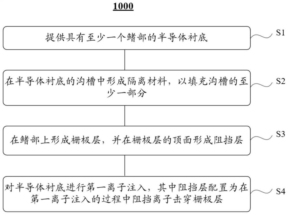
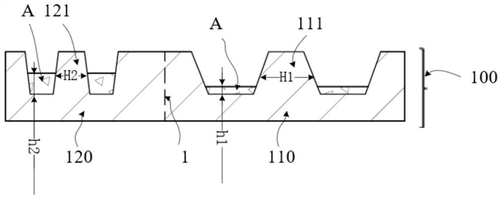
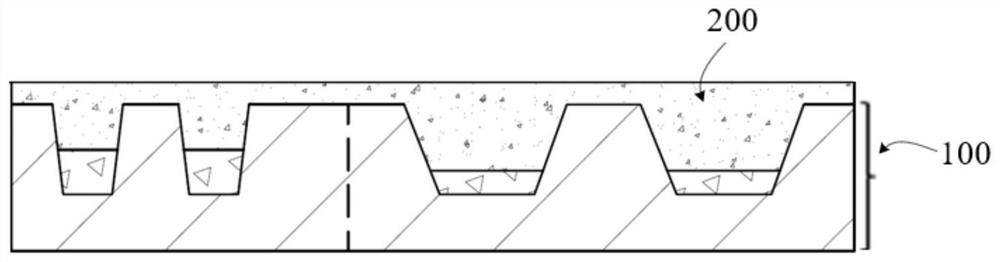
[0042] For a better understanding of the application, various aspects of the application will be described in more detail with reference to the accompanying drawings. It should be understood that these detailed descriptions are descriptions of exemplary embodiments of the application only, and are not intended to limit the scope of the application in any way.

[0043] The terminology used herein is for the purpose of describing particular exemplary embodiments and is not intended to be limiting. When used in this specification, the terms "comprises", "includes", "includes" and / or "includes" indicate the presence of said features, integers, elements, components and / or combinations thereof, but do not exclude The presence of one or more other features, integers, elements, components and / or combinations thereof.

[0044] The description herein is made with reference to schematic illustrations of exemplary embodiments. Exemplary embodiments disclosed herein should not be constru...


PUM


Abstract

The invention provides a three-dimensional memory and a preparation method thereof. The preparation method of the three-dimensional memory comprises the steps of providing a semiconductor substrate with at least one fin part; forming an isolation material in a trench of the semiconductor substrate to fill at least a part of the trench; forming a gate layer on the fin part, and forming a barrier layer on the top surface of the gate layer; and performing first ion implantation on the semiconductor substrate, wherein the barrier layer is configured to prevent ions from puncturing the gate layer in the first ion implantation process.

Description

technical field [0001] The present application relates to the technical field of semiconductors, and more specifically, to a three-dimensional memory and a manufacturing method thereof. Background technique [0002] At present, in the peripheral process of a three-dimensional memory (3D NAND) based on the X-tacking architecture, as the number of stacked layers increases, the requirements for the area of ​​the MOS region (such as the CMOS region) become more and more stringent. In order to reduce the area of ​​the MOS region, many 3D NAND manufacturers adopt the X-FET process, which is to make the planar storage device into a three-dimensional storage device. [0003] Although the area of ​​the MOS region can be greatly reduced by applying the X-FET process to the 3D NAND MOS process, with the development of the semiconductor technology field, the performance requirements of MOS devices under the X-FET process in the market also gradually increased. For example, under the t...

Claims


Application Information

Patent Timeline
IPC IPC(8): H01L27/11524H01L27/11529H01L27/11531H01L27/11551H01L27/1157H01L27/11573H01L27/11578
CPCH10B41/41H10B41/35H10B41/42H10B41/20H10B43/35H10B43/20H10B43/40
Inventor 黄腾华子群石艳伟姚兰
Owner YANGTZE MEMORY TECH CO LTD
Why Eureka
Try Eureka