MEMS device manufacturing method and MEMS device

A device manufacturing method and device technology, applied in semiconductor/solid-state device components, electric solid-state devices, semiconductor devices, etc., can solve the problems that it is difficult to ensure that the organic film is not damaged, the etching effect is difficult to ensure, and the process is complicated. Achieve the effects of reduced manufacturing cost, clean removal effect, and simplified process links

Pending Publication Date: 2021-12-03
SEMICON MFG ELECTRONICS (SHAOXING) CORP
View PDF1 Cites 2 Cited by
  • Summary
  • Abstract
  • Description
  • Claims
  • Application Information

AI Technical Summary

Problems solved by technology

This process of patterning the organic film needs to be completed in two steps. The process is relatively complicated and there are many procedures. The organic film on the surface of the electrode layer needs to be removed by a wet etching process, which requires photolithography to open windows, and the etching effect is difficult to guarantee. And it is difficult to guarantee that the organic film in other areas will not be damaged

Method used


Image

  • MEMS device manufacturing method and MEMS device
  • MEMS device manufacturing method and MEMS device
  • MEMS device manufacturing method and MEMS device

Examples


Embodiment Construction

[0020] The following will clearly and completely describe the technical solutions in the embodiments of the present invention with reference to the drawings in the embodiments of the present invention.

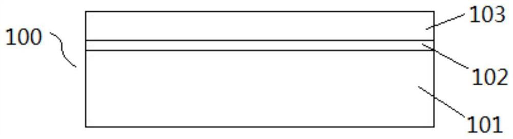
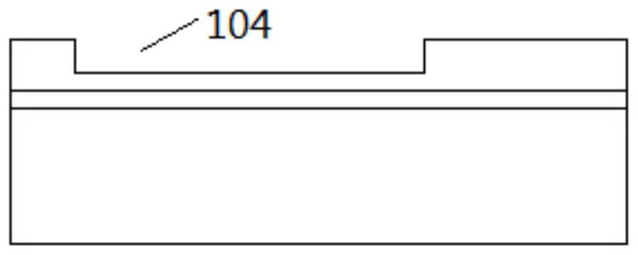
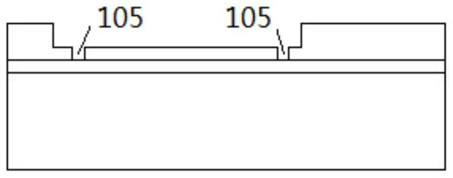
[0021] This embodiment discloses a MEMS device and a MEMS device manufacturing method. By adjusting the structure and process method of the existing MEMS device, it mainly solves the problem of removing the hydrophobic organic film used to eliminate the adhesion phenomenon on the surface of the bonding area and the electrode area. Difficult technical problem, optimize the design of the patterning method of the existing hydrophobic organic film, aim to simplify the process link, make it easier to implement technically, reduce the manufacturing cost, and ensure that the method can integrate the surface of the bonding area and the electrode area The hydrophobic organic film is removed cleanly, improving the reliability of bonding and the reliability of electrode lead wire bonding....


PUM


Abstract

The invention relates to an MEMS device manufacturing method and an MEMS device, an SOI insulator silicon wafer is selected as a substrate, and silicon-silicon bonding is carried out through SOI top silicon and a silicon wafer serving as a structural layer, so that the whole manufacturing process can be compatible with a VHF process; before the hydrophobic organic film is formed, a layer of sacrificial layer silicon dioxide is deposited in the area where the hydrophobic organic film needs to be removed, and after the hydrophobic organic film is formed, the silicon dioxide sacrificial layer on the bonding area and the electrode area can be etched off by means of the VHF technology. The hydrophobic organic films on the bonding area and the electrode area are removed while the silicon dioxide is removed, and the hydrophobic organic films needing to be reserved in other areas are not affected. The manufacturing method disclosed by the invention is simple in process and high in feasibility, the hydrophobic organic films on the bonding region and the electrode region can be removed completely at the same time, and the hydrophobic organic films reserved in other regions cannot be damaged.

Description

technical field [0001] The invention relates to the technical field of semiconductor manufacturing, in particular to a MEMS device manufacturing method and the MEMS device. Background technique [0002] MEMS refers to a micro-electromechanical system that integrates micro sensors, actuators, signal processing and control circuits, interface circuits, communications and power supplies. Micro-sensors, micro-actuators, micro-components, micro-mechanical optical devices, vacuum microelectronic devices, power electronic devices, etc. made by MEMS technology have very broad applications in aerospace, automotive, biomedicine, environmental monitoring, military and other fields. Application prospect. Common MEMS devices currently on the market include pressure sensors, magnetic sensors, microphones, accelerometers, gyroscopes, infrared sensors, etc. [0003] MEMS devices have a large surface / volume ratio, and this structure is prone to wear / adhesion between structural layers durin...

Claims


Application Information

Patent Timeline
Patent Type & Authority Applications(China)
IPC IPC(8): B81C1/00B81B7/00B81B7/02
CPCB81B7/0058B81C1/00261B81B7/02B81C2203/01
Inventor 王新龙
Owner SEMICON MFG ELECTRONICS (SHAOXING) CORP
Why Eureka
Try Eureka