Semiconductor structure and forming method thereof

A technology of semiconductor and gate structure, applied in the field of semiconductor structure and its formation, can solve the problems of poor control ability of gate structure and difficult channel, so as to alleviate short channel effect, improve electrical performance, reduce short channel Dow effect

Pending Publication Date: 2021-12-07
SEMICON MFG INT (SHANGHAI) CORP +1
View PDF0 Cites 0 Cited by
  • Summary
  • Abstract
  • Description
  • Claims
  • Application Information

AI Technical Summary

Problems solved by technology

However, with the shortening of the channel length of the device, the distance between the source region and the drain region of the device is also shortened, so the control ability of the gate structure on the channel becomes worse, and the gate voltage pinches off the channel. The difficulty is also increasing, making the phenomenon of subthreshold leakage (subthreshold leakage), the so-called short-channel effects (short-channel effects, SCE) more prone to occur

Method used


Image

  • Semiconductor structure and forming method thereof
  • Semiconductor structure and forming method thereof
  • Semiconductor structure and forming method thereof

Examples


Embodiment Construction

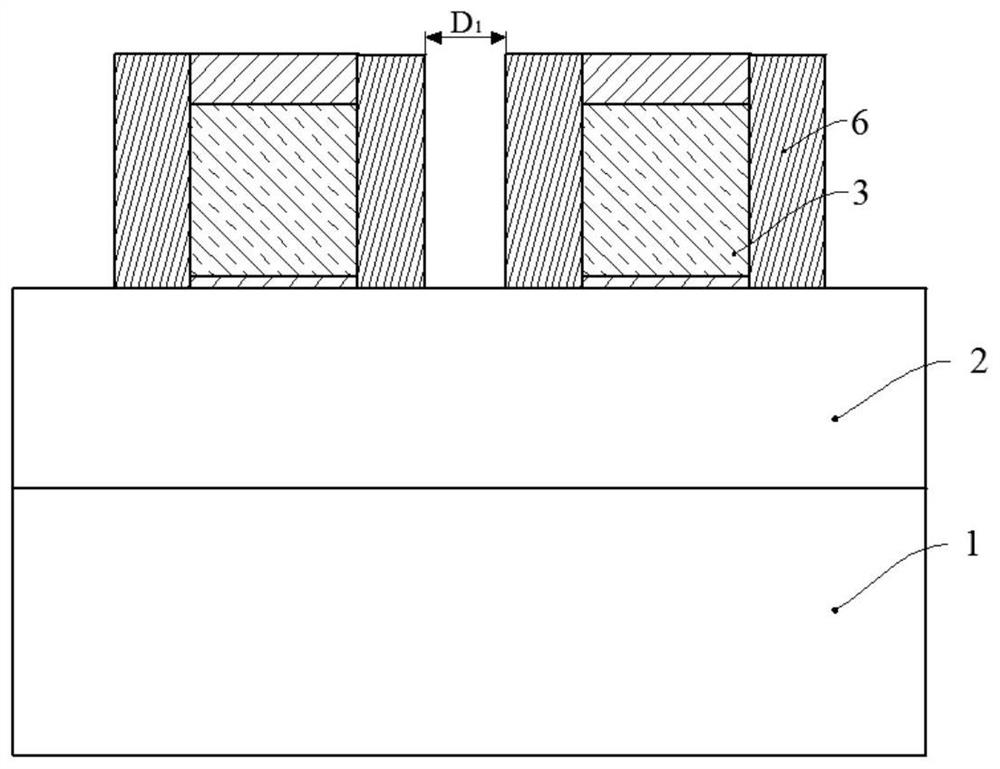
[0029] It can be seen from the background art that the devices formed so far still have the problem of poor performance. The reasons for the poor performance of the device are analyzed in conjunction with a method of forming a semiconductor structure.

[0030] Figure 1 to Figure 3 A structural schematic diagram corresponding to each step in a method for forming a semiconductor structure is shown.

[0031] like figure 1 As shown, a base is provided, the base includes a substrate 1, a fin 2 on the substrate 1, and a gate structure 3 across the fin 2, and the gate structure 3 covers the fin Part of the top wall and part of the side wall of the part 2; a side wall layer 6 is formed on the side wall of the gate structure 3, and the size between the side wall layers 6 on the side wall of the adjacent gate structure 3 as D 1 .

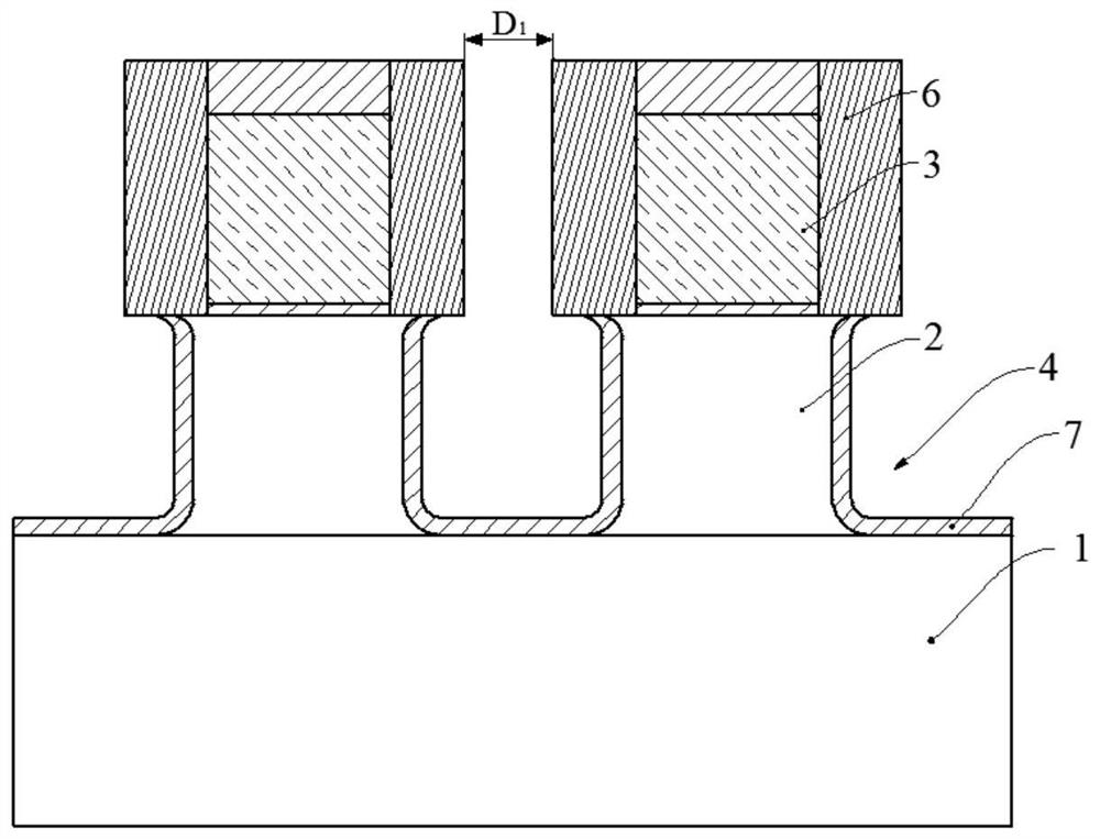
[0032] like figure 2 As shown, the fins 2 on both sides of the gate structure 3 are etched to form a groove 4 in the fin 2; an anti-diffusion layer 7...


PUM

PropertyMeasurementUnit
Horizontal sizeaaaaaaaaaa

Abstract

The invention discloses a semiconductor structure and a forming method thereof, and the method comprises the steps of providing a substrate and a gate structure located on the substrate, and taking an extension direction which is parallel to the surface of the substrate and is perpendicular to the gate structure as a transverse direction; forming a first side wall material layer on the side wall of the gate structure; forming a groove in the substrate at the two sides of the gate structure and the first side wall material layer; in the transverse direction, thinning the first side wall material layer, and forming a first side wall layer; forming an anti-diffusion region on the side wall and the bottom surface of the groove; and forming a source-drain doping layer in the groove. In the embodiment of the invention, the transverse size of the groove exposed by the first side wall layer is larger, a larger process window is provided for forming the anti-diffusion region, so that the anti-diffusion region can better prevent the first-type ions in a source-drain doping layer from diffusing into a channel below the gate structure; and when the semiconductor structure works, a depletion region of the source-drain doping layer is not easy to expand, and the electrical performance of the semiconductor structure can be improved.

Description

technical field [0001] Embodiments of the present invention relate to the field of semiconductor manufacturing, and in particular, to a semiconductor structure and a method for forming the same. Background technique [0002] In semiconductor manufacturing, with the development trend of ultra-large-scale integrated circuits, the feature size of integrated circuits continues to decrease. In order to adapt to smaller feature sizes, metal-oxide-semiconductor field-effect transistors (Metal-Oxide-Semiconductor Field-Effect Transistor , MOSFET) channel length has been shortened accordingly. However, as the channel length of the device is shortened, the distance between the source region and the drain region of the device is also shortened, so the control ability of the gate structure to the channel becomes worse, and the gate voltage pinches off the channel. Difficulty is also increasing, making subthreshold leakage (subthreshold leakage), the so-called short-channel effects (sho...

Claims


Application Information

Patent Timeline
IPC IPC(8): H01L21/336H01L29/78H01L29/08H01L21/8234H01L27/088
CPCH01L29/66795H01L29/785H01L29/0847H01L21/823418H01L21/823431H01L21/823468H01L27/0886
Inventor 赵猛施雪捷
Owner SEMICON MFG INT (SHANGHAI) CORP
Why Eureka
Try Eureka