Composite double-gate high-speed PMOS device based on Ga2O3 material and production method of composite double-gate high-speed PMOS device

A compound, high-speed technology, applied in semiconductor/solid-state device manufacturing, semiconductor devices, electrical components, etc., can solve problems such as insufficient hole transport rate, low thermal conductivity, and affecting device performance, and achieve the reduction of short channel effect, high transconductance, and high carrier mobility

Active Publication Date: 2017-02-22
XIDIAN UNIV
View PDF4 Cites 3 Cited by
  • Summary
  • Abstract
  • Description
  • Claims
  • Application Information

AI Technical Summary

Problems solved by technology

[0005] The current third-generation wide-bandgap semiconductor material Ga 2 o 3 The PMOS device of the material is an emerging research direction as a semiconductor integrated circuit power device and an optoelectronic device, but due to the β-Ga 2 o 3 When the substrate is applied to high-speed devices, there are disadvantages such as insufficient hole transport rate and low thermal conductivity compared with other wide-bandgap materials. In addition, the metal gate / high-k gate dielectric structure is applied to Ga 2 o 3 The serious Fermi pinning effect appears on the substrate, which greatly affects the Ga 2 o 3 Device Performance of PMOS Devices

Method used


Image

  • Composite double-gate high-speed PMOS device based on Ga2O3 material and production method of composite double-gate high-speed PMOS device
  • Composite double-gate high-speed PMOS device based on Ga2O3 material and production method of composite double-gate high-speed PMOS device
  • Composite double-gate high-speed PMOS device based on Ga2O3 material and production method of composite double-gate high-speed PMOS device

Examples


Embodiment 1

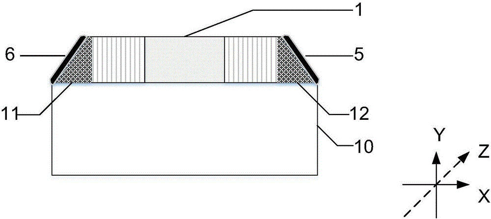
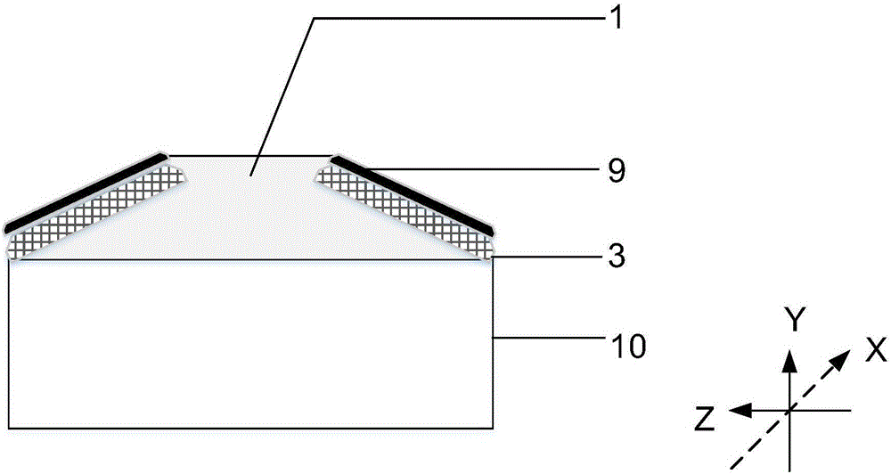
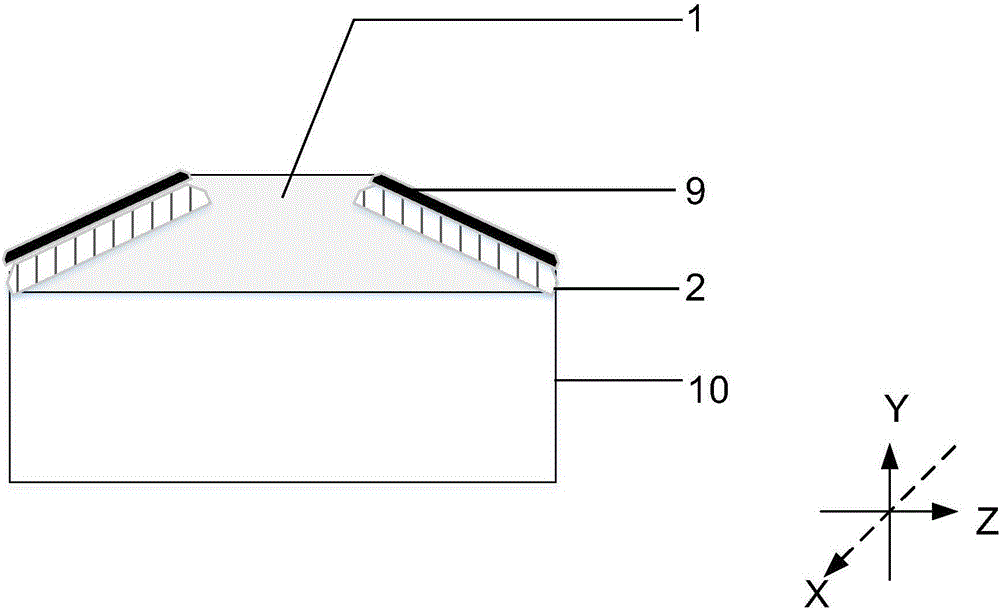
[0047] See figure 1 , figure 2 , image 3 and Figure 4 , figure 1 A Ga-based 2 o 3 The first cross-sectional schematic diagram of the composite double-gate high-speed PMOS device of the material (taken along the plane formed by the XY axis), figure 2 A Ga-based 2 o 3 The second cross-sectional schematic diagram of the compound double-gate high-speed PMOS device of the material (intercepted along the plane formed along the ZY axis, and the viewing angle is: the direction of the drain electrode → source electrode), image 3 A Ga-based 2 o 3 The third cross-sectional schematic diagram of the composite double-gate high-speed PMOS device of the material (taken along the plane formed along the ZY axis, and the viewing angle is: the direction of the source electrode → the drain electrode), Figure 4 A Ga-based 2 o 3 A schematic top view of a composite double-gate high-speed PMOS device made of materials. The composite double-gate high-speed PMOS device includes a gall...

Embodiment 2

[0076] Please also see Figure 6a-6j , Figures 7-10, Figure 6a-6j A Ga-based 2 o 3 A schematic diagram of the preparation method of a composite double-gate high-speed PMOS device; FIG. 7 is a schematic structural diagram of a first mask set provided by an embodiment of the present invention; FIG. 8 is a second mask provided by an embodiment of the present invention Figure 9 is a schematic structural view of a third mask provided by an embodiment of the present invention; Figure 10 is a schematic structural view of a fourth mask provided by an embodiment of the present invention; and Figure 11a-Figure 11d A schematic structural diagram of a fifth mask set provided by an embodiment of the present invention. On the basis of the above-mentioned embodiments, this embodiment is based on the Ga 2 o 3 The preparation method of the composite double-gate high-speed PMOS device of the material is described in detail as follows:

[0077] Step 1: See Figure 6a , prepare a semi-in...


PUM

PropertyMeasurementUnit
Thicknessaaaaaaaaaa
Thicknessaaaaaaaaaa

Abstract

The invention relates to a composite double-gate high-speed PMOS device based on a Ga2O3 material and a production method of the composite double-gate high-speed PMOS device. The method includes: selecting an N type semi-insulating substrate, and using molecular beam epitaxy to grow an N type beta-Ga2O3 layer; using dry etching to form a mesa, and using an ion implantation process to form a source region and a drain region on two sides of the mesa; forming a source and a drain at the two slope positions, located at the source region and the drain region, of the N type beta-Ga2O3 substrate; using a magnetron sputtering process to form a first gate medium layer at the other two slopes, close to the source region, of the N type beta-Ga2O3 mesa; using a magnetron sputtering process to form a second gate medium layer at the other two slopes, close to the drain region, of the N type beta-Ga2O3 substrate so as to form a composite double-gate medium layer; forming a gate on the surface of the composite double-gate medium layer. The composite double-gate high-speed PMOS device based on the Ga2O3 material has the advantage that two materials of different dielectric constants are used as the composite gate oxide layer to transmit hole-blocking electrons so as to increase transmission rate.

Description

technical field [0001] The invention belongs to the technical field of integrated circuits, in particular to a Ga-based 2 o 3 A composite double-gate high-speed PMOS device of the material and a preparation method thereof. Background technique [0002] MOS devices, that is, metal-oxide-semiconductor field effect transistors, have been completely different in structure and performance from the previous bipolar integrated circuits since their inception. MOS integrated circuits have high input impedance, strong anti-interference ability, low power consumption, The advantages of high integration and so on have become the mainstream of the VLSI era. MOS devices are divided into NMOS, PMOS, and CMOS according to different substrates and different conductive channels. Among them, MOS devices that use N-type substrates to form P-type channels are PMOS. [0003] PMOS is turned on after Vgs is less than a fixed value. The carrier that the current transmission of the device depends ...

Claims


Application Information

Patent Timeline
IPC IPC(8): H01L21/336H01L21/28H01L29/423
CPCH01L21/28008H01L29/42364H01L29/66477
Inventor 元磊张弘鹏贾仁需张玉明
Owner XIDIAN UNIV
Why Eureka
Try Eureka