Gate-last ferroelectric field effect transistor and manufacturing method thereof
Pending Publication Date: 2022-01-20
XIANGTAN UNIV
View PDF0 Cites 0 Cited by
Summary
Abstract
Description
Claims
Application Information
AI Technical Summary
This helps you quickly interpret patents by identifying the three key elements:
Problems solved by technology
Method used
Benefits of technology
Benefits of technology
This patent describes a technique for improving the performance and reducing the power consumption of a type of electronic device called a gate-last ferroelectric field effect transistor. The technique involves using a multi-layer metal gateelectrode with lightly doped drain regions to reduce the short channel effect of the device and increase its integration level. Additionally, a dummy gate is used to manufacture a hafnium oxide-based ferroelectric field effect transistor with an improved response speed and reliability. The manufacturing process is simplified by using a single RTA process which simultaneously crystallizes the hafnium oxide-doped film layer and activates the implanted ions to form the source / drain region of the device. Furthermore, a metal silicide is formed on the source / drain region to lower its contact resistance. Overall, the patent provides a technical solution for improving the performance and reducing the power consumption of gate-last ferroelectric field effect transistors.
Problems solved by technology
The main limiting factors are: 1) the traditional ferroelectric thin films with the perovskite structure is incompatible with a standard complementary metaloxidesemiconductor (CMOS) process; 2) when the ferroelectric film has a thickness less than 50 nm, the properties of the ferroelectric film are seriously degraded; and 3) the integration process is complicate.
However, the above methods have the following shortcomings: firstly, TiN and TaN electrodes are quite likely to react with hafnium oxide-based films to form interface layers, which increases oxygen vacancies in the films, thus affecting an electrical reliability of a device; secondly, metal elements may be diffused, which also affects the electrical reliability of the devices; and thirdly, it is difficult to regulate or control a threshold voltage of the hafnium oxide-based ferroelectric field effect transistor.
Method used
Image
Click on the blue label to locate the original text in one second.
Reading with bidirectional positioning of images and text.
[0102]Referring to FIG. 2-8, in a specific embodiment of the present disclosure, a manufacturing method of the present disclosure is used to manufacture a gate-last hafnium oxide-based ferroelectric field effect transistor, where the gate-last hafnium oxide-based ferroelectric field effect transistor includes:
[0104]isolation regions 2 symmetrically arranged at two ends of the substrate 1, wherein upper surfaces of the isolation regions 2 are not lower than that of the substrate 1, bottom surfaces of the isolation regions 2 are higher than that of the substrate 1, and the isolation regions are made from SiO2;
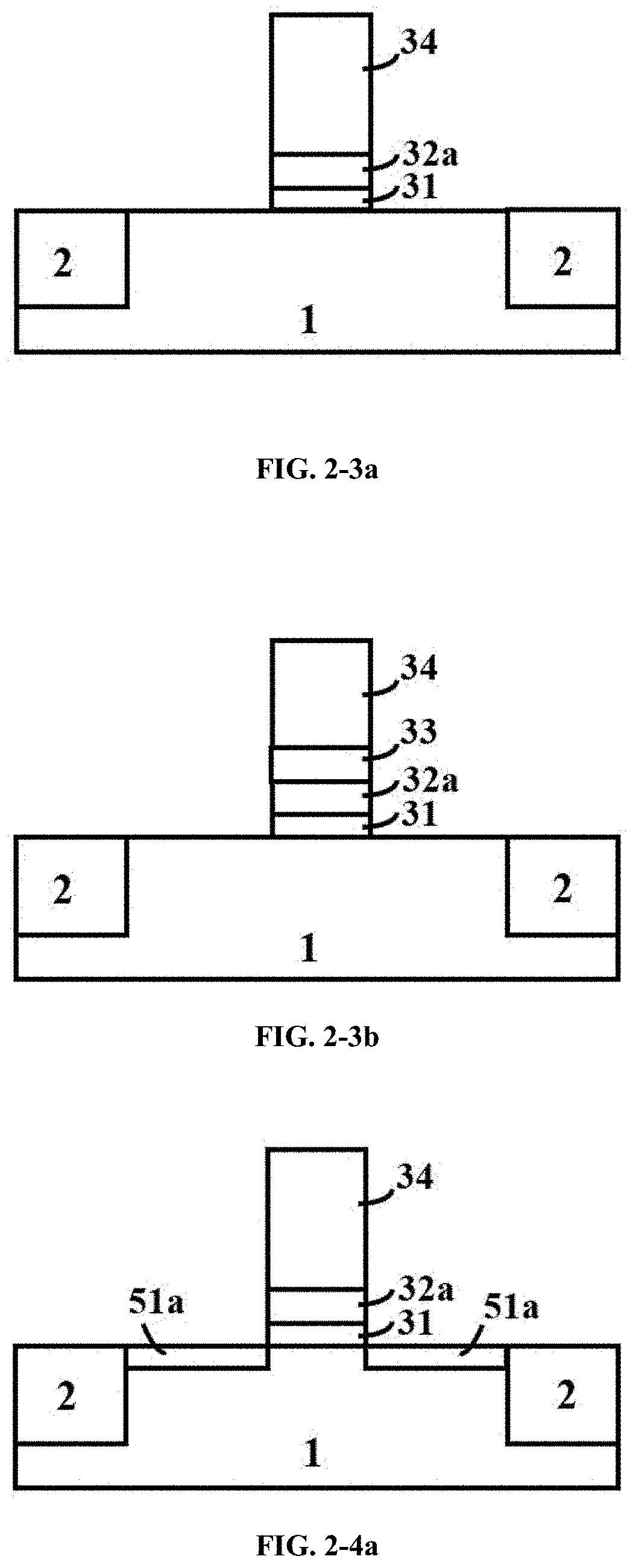
[0105]a gate structure 3, which includes a buffer layer 31, a doped hafnium oxide-based ferroelectric film layer 32b, a gate electrode layer 8 and a metal layer 9 which are sequent...
embodiment 2
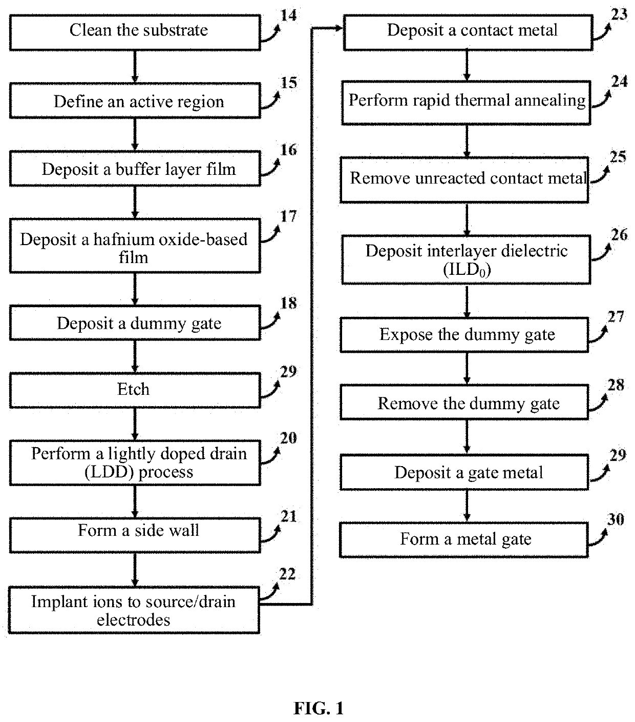
[0110]Referring to FIG. 1, a manufacturing method of a gate-last hafnium oxide-based ferroelectric field effect transistor of the present disclosure is as follows by taking p-type monocrystalline silicon (p-Si) as an example:
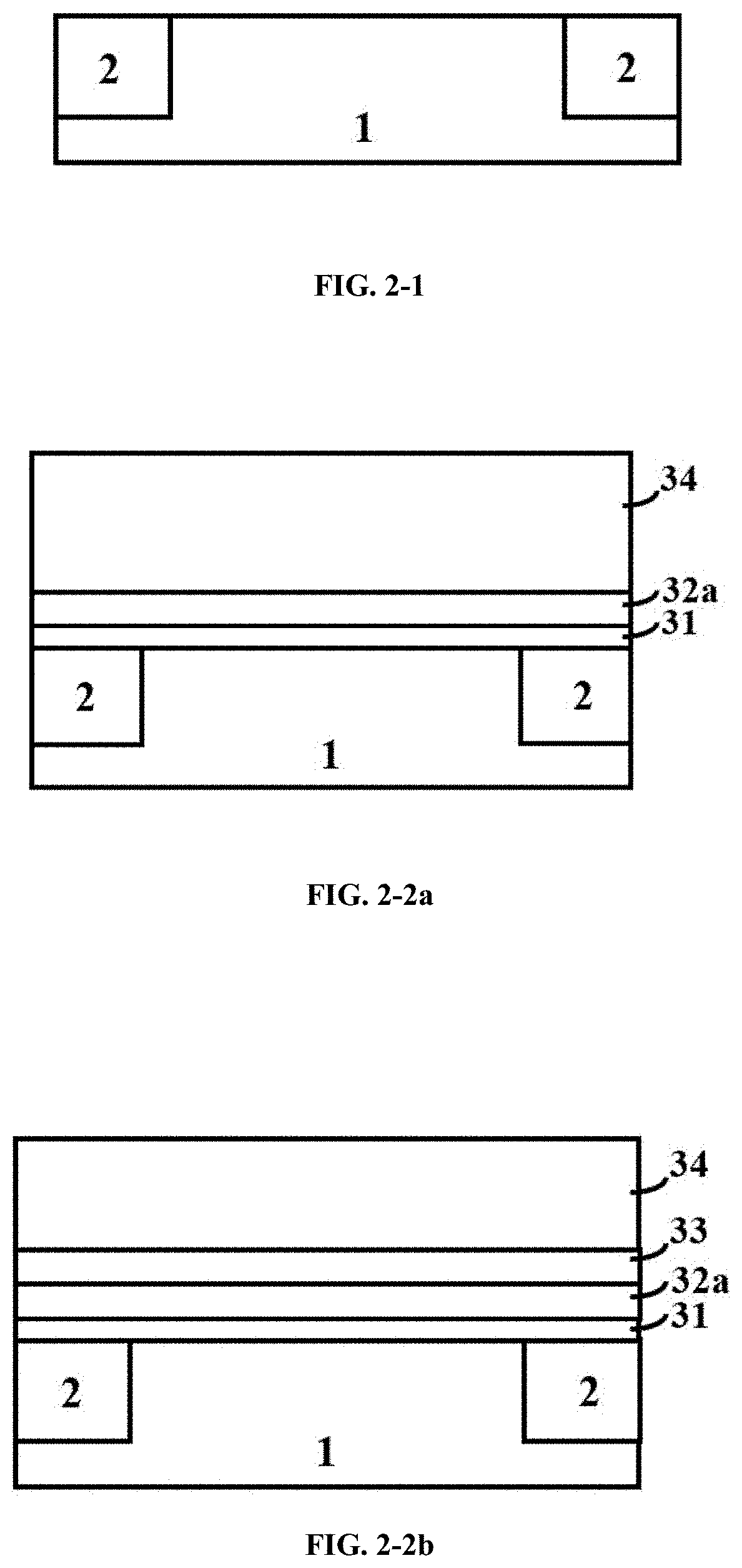
[0111]S1, referring to FIG. 1 and FIG. 2-1, firstly, the substrate 1 is cleaned by a standard cleaning process according to a process flow 14;
[0112]S2, an active region is defined according to a process flow 15; the isolation regions 2 are formed by a local oxidation of silicon (LOCOS) process; the other regions are considered as the active region;
[0113]S3, referring to FIG. 1 and FIG. 2-2a, firstly, the substrate is cleaned again by the standard cleaning process to remove an oxide layer from a surface of the active region, and a buffer layer 31 made from SiO2 and with a thickness of 1 nm is formed on the substrate by a chemical oxidization process according to a process flow 16;
[0114]S4, referring to FIG. 1 and FIG. 2-2a, a hafnium oxide-doped film layer 32a wi...
embodiment 3
[0127]Referring to FIG. 1, a manufacturing method of a gate-last hafnium oxide-based ferroelectric field effect transistor of the present disclosure is as follows by taking a p-type silicon-on-insulator (SOI) as an example:
[0128]S1, referring to FIG. 1 and FIG. 2-1, firstly, the substrate 1 is cleaned by a standard cleaning process according to a process flow 14;
[0129]S2, an active region is defined according to a process flow 15, namely the substrate 1 is etched by a reactive ion etching process to form a Mesa structure to form isolation regions 2, and the other regions are considered as active regions;
[0130]S3, referring to FIG. 1 and FIG. 2-2a, firstly, the substrate is cleaned again by the standard cleaning process to remove an oxide layer on a surface of the active region; a SiON buffer layer 31 with a thickness of 3 nm is deposited on the substrate by a thermal oxidation process according to a process flow 16; the thermal oxidation process includes the operations of: firstly, ...
PUM
Abstract
A gate-last ferroelectric field effecttransistor includes a substrate, isolation regions, a gate structure, a side wall spacer, source and drain regions, a first metalsilicide layer and an interlayer dielectric layer which are sequentially arranged from bottom to top; the present disclosure further provides a manufacturing method of a gate-last ferroelectric field effecttransistor; according to structural characteristics of the gate-last ferroelectric field effecttransistor and crystalline characteristics of a hafniumoxide-based ferroelectric film, a dummy gate is first introduced in a manufacturing process of the gate-last ferroelectric field effect transistor; afterwards, high-temperature annealing is performed to make sure that an unannealed hafniumoxide-based film is crystallized to form a ferroelectric phase; finally the dummy gate is removed and a gate electrode layer is deposited to meet performance requirements of the gate-last ferroelectric field effect transistor; and the gate-last ferroelectric field effect transistor has an excellent application prospect.
Description
CROSS REFERENCE TO RELATED APPLICATIONS[0001]The application is a continuation of International Patent Application No. PCT / CN2019 / 080758 with a filing date of Apr. 1, 2019, designating the United States, now pending, and further claims the priority to Chinese Patent Application No. 201910234444.4 with a filing date of Mar. 26, 2019. The content of the aforementioned applications, including any intervening amendments thereto, are incorporated herein by reference.TECHNICAL FIELD[0002]The present disclosure relates to the technical field of electronic elements, in particular to a gate-last ferroelectric field effect transistor and a manufacturing method thereof.BACKGROUND[0003]As an important leading edge and a research hotspot of high information technologies at present, ferroelectric memory is considered as one of the most potential memories in the next generation of memories due to its advantages such as non-volatility, low power consumption, high endurance, fast read and write spee...
Claims
Application Information
Patent Timeline
Application Date:The date an application was filed.
Publication Date:The date a patent or application was officially published.
First Publication Date:The earliest publication date of a patent with the same application number.
Issue Date:Publication date of the patent grant document.
PCT Entry Date:The Entry date of PCT National Phase.
Estimated Expiry Date:The statutory expiry date of a patent right according to the Patent Law, and it is the longest term of protection that the patent right can achieve without the termination of the patent right due to other reasons(Term extension factor has been taken into account ).
Invalid Date:Actual expiry date is based on effective date or publication date of legal transaction data of invalid patent.

