

Semiconductor device and manufacturing method of the same
- Summary
- Abstract
- Description
- Claims
- Application Information
AI Technical Summary
Benefits of technology
Problems solved by technology
Method used
Image

Examples
first embodiment
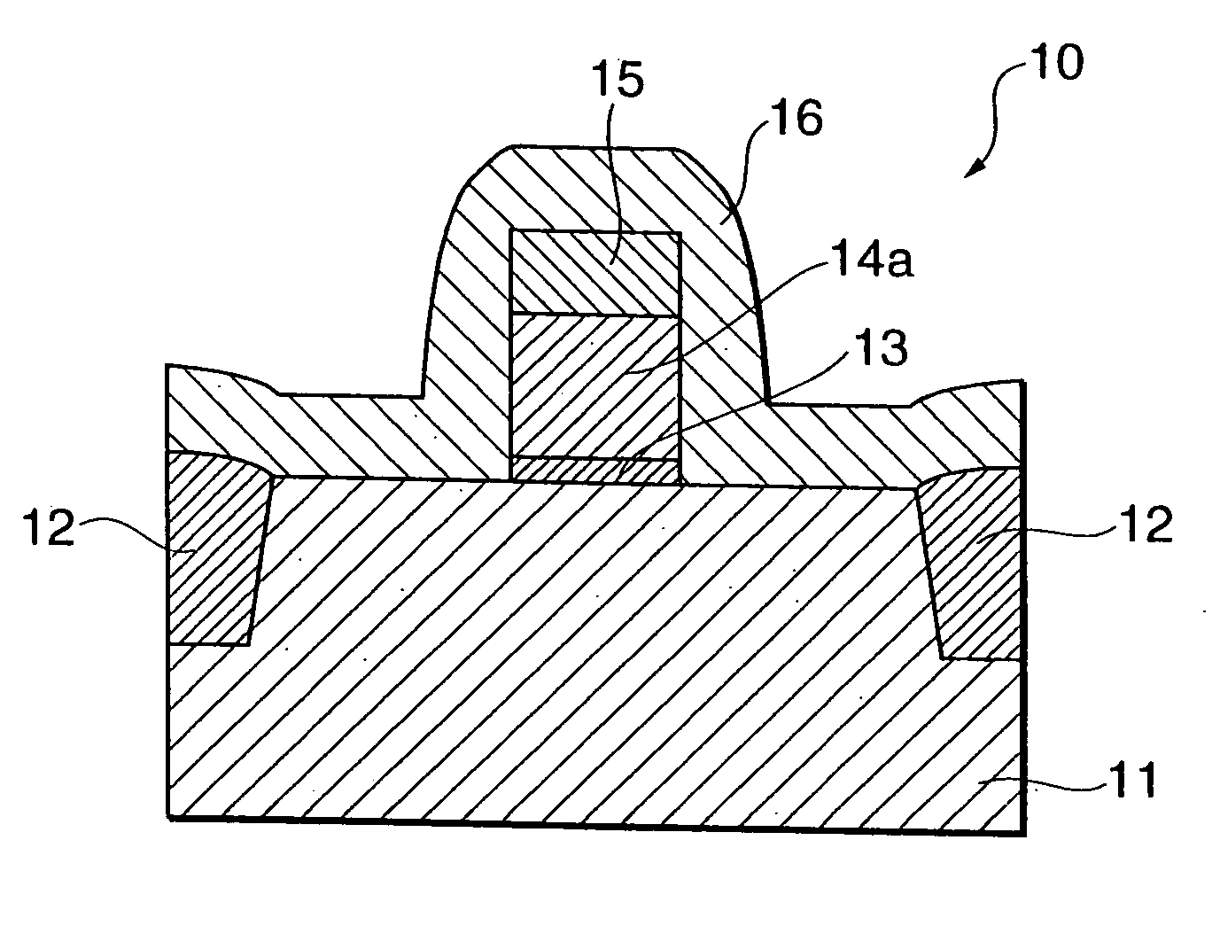
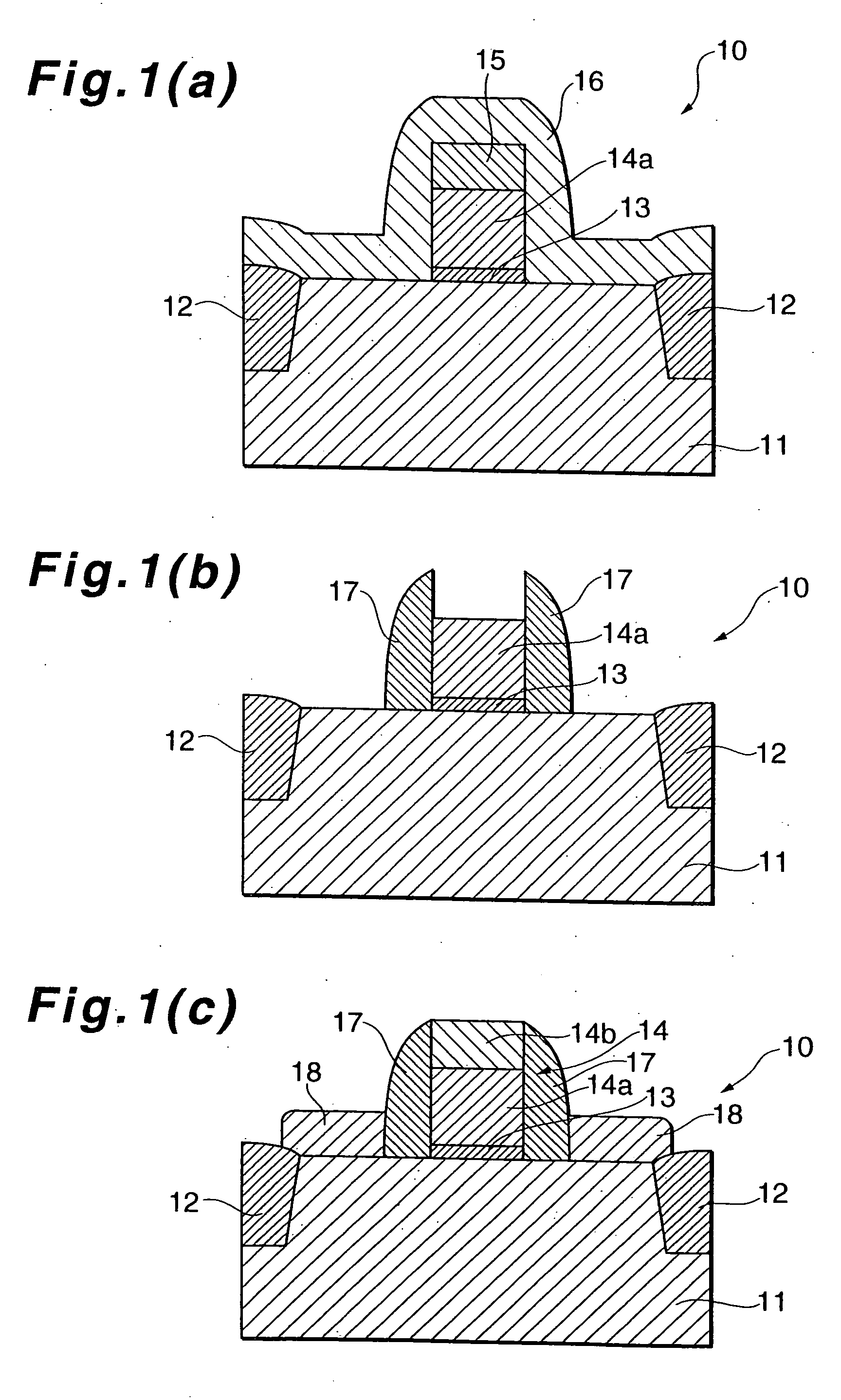
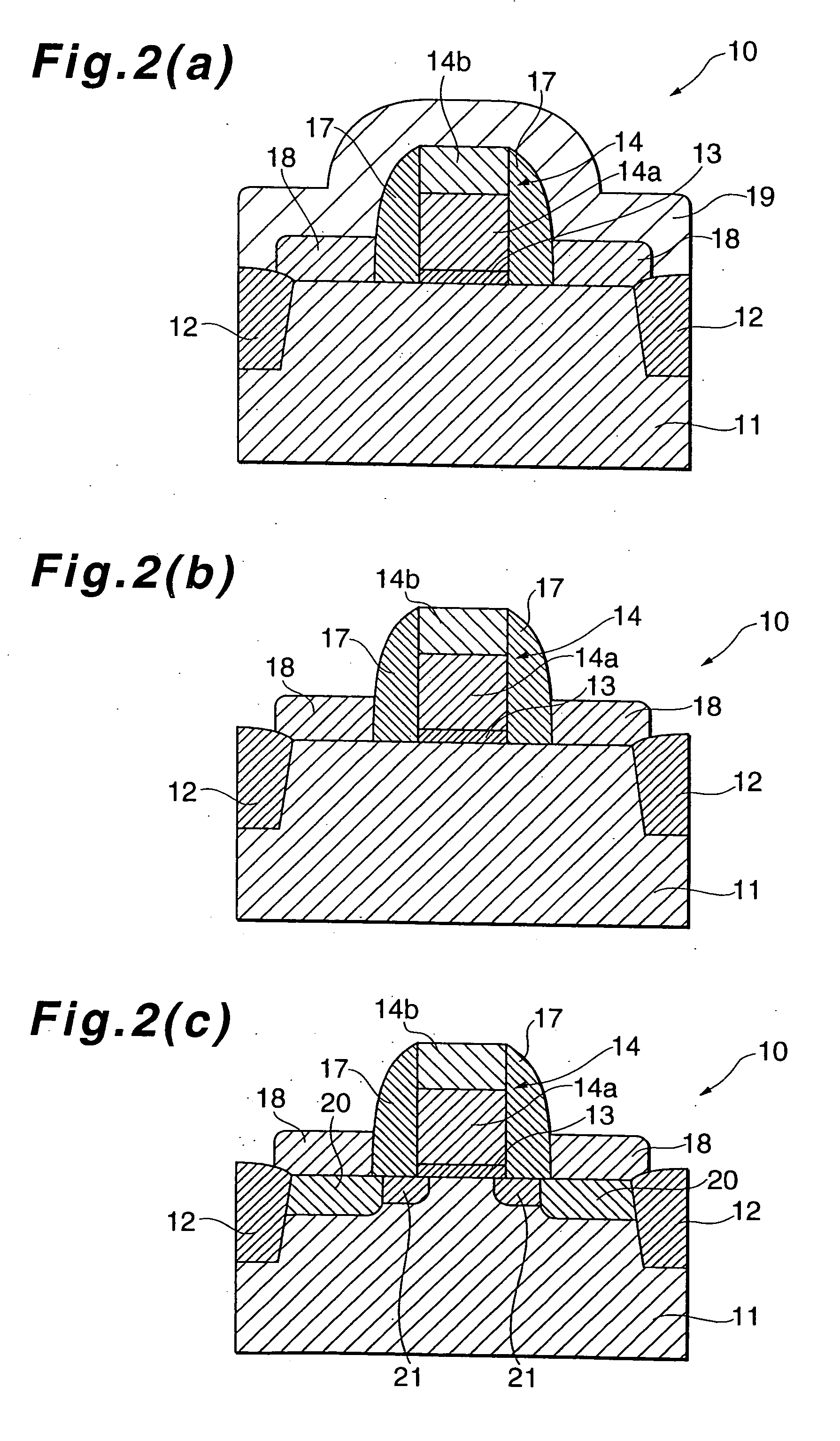
[0046]FIG. 1(a), (b) and (c) and FIG. 2(a), (b) and (c) are diagrams showing processes of manufacturing a semiconductor device 10 according to a first embodiment of the present invention. In FIG. 1(a), (b) and (c) and FIG. 2(a), (b) and (c) is shown a process of manufacturing an n-channel MOS FET using, for example, a p-type substrate.
[0047] As shown in FIG. 1(a), on a silicon semiconductor substrate exhibiting a p-type characteristic, as is well known, is formed a device separating region 12 to partition an active region for a semiconductor device. The device separating region 12 is formed by an STI (Shallow Trench Isolation) method.
[0048] On the active region partitioned by the device separating region 12 is formed a gate electrode 14 used for the MOS FET. The gate electrode 14 includes a gate electrode member 14a formed on the active region with a gate insulator 13 interposed therebetween. To form the gate electrode 14, as is well known, on the active region are sequentially st...
second embodiment
[0064] In the process of manufacturing a semiconductor device 10 of a second embodiment of the present invention, as shown in FIG. 3(a) to FIG. 3(d), after a pair of the source / drain electrode members 18 has been formed, a gate electrode 14 is formed.
[0065] As shown in FIG. 3(a), on a silicon semiconductor substrate 11 exhibiting a p-type characteristic is formed a device separating region 12 having the same structure as in the first embodiment. A silicon layer 22 with a thickness of 50 nm to be used as electrodes to be used for a source and a drain is formed on the active region partitioned by the device separating region 12. Then, a cobalt layer 19 is formed in a manner that it covers the device separating region 12 and the silicon layer 22. The cobalt layer 19 is formed by the well-known sputtering method so as to have the thickness of 50 nm. Moreover, to introduce an impurity into the cobalt layer, the n-type impurity such as phosphorous is implanted by the ion implantation met...
PUM
 Abstract
Description
Claims
Application Information