Manufacturing method of MOS (metal oxide semiconductor) transistor

A technology of MOS transistors and manufacturing methods, which is applied in the manufacture of semiconductor/solid-state devices, electrical components, circuits, etc., can solve the problems of low junction capacitance and junction leakage performance, inability to meet the requirements, and achieves the reduction of junction capacitance, junction leakage, and reduction. Effects of small short channel effects

Active Publication Date: 2013-01-30
SEMICON MFG INT (SHANGHAI) CORP
View PDF4 Cites 2 Cited by
  • Summary
  • Abstract
  • Description
  • Claims
  • Application Information

AI Technical Summary

Problems solved by technology

The further reduction of device feature size requires the formation of shallower ultra-shallow junctions in device manufacturing, and devices have lower junction capacitance and junction leakage performance. The above-mentioned processes have been unable to meet the requirements of device manufacturing.

Method used


Image

  • Manufacturing method of MOS (metal oxide semiconductor) transistor
  • Manufacturing method of MOS (metal oxide semiconductor) transistor
  • Manufacturing method of MOS (metal oxide semiconductor) transistor

Examples


Embodiment Construction

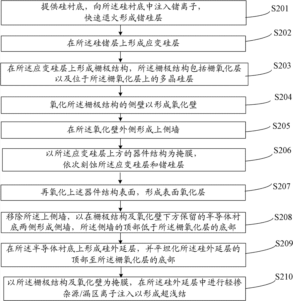
[0043] The present invention proposes a kind of manufacturing method of MOS transistor, and this method comprises the following steps:

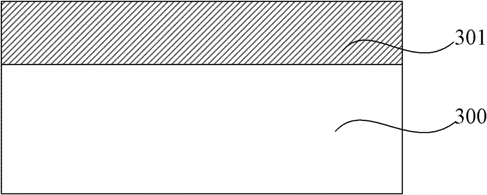
[0044] Provide semiconductor substrates;

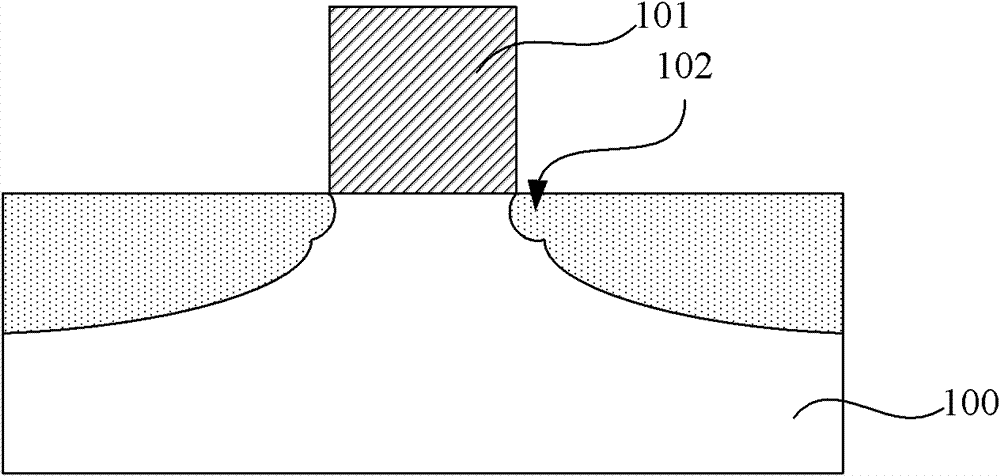
[0045] forming a gate structure on the semiconductor substrate, the gate structure comprising a gate oxide layer and a polysilicon layer on the gate oxide layer;

[0046] oxidizing sidewalls of the gate structure to form oxide walls;

[0047] using the gate structure and the oxide wall as a mask to remove part of the semiconductor substrate;

[0048] re-oxidizing the remaining upper surface of the semiconductor substrate to form a surface oxide layer;

[0049] Etching the surface oxide layer to form sidewalls on both sides of the semiconductor substrate remaining under the gate structure and the oxide wall, the top of the sidewalls is lower than the bottom of the gate oxide layer;

[0050] forming a silicon epitaxial layer on the semiconductor substrate, and planarizing the top of the silicon epit...


PUM

PropertyMeasurementUnit
Feature sizeaaaaaaaaaa
Thicknessaaaaaaaaaa
Thicknessaaaaaaaaaa

Abstract

The invention provides a manufacturing method of an MOS (metal oxide semiconductor) transistor. A side wall of which the top is lower than the bottom of a grid oxide layer is utilized to inhibit the radial diffusion of the lightly doped source / drain (LDD) after ion implantation and control the depth of the formed LDD extension zone, so that the obtained ultra-shallow junction is more shallow, thereby reducing the short channel effect and lowering the junction capacitance; and further more, a strain silicon layer and a germanium silicon layer are utilized to increase the charge migration rate and lower the junction capacitance and junction leakage.

Description

technical field [0001] The invention relates to the field of semiconductor manufacturing, in particular to a method for manufacturing a MOS transistor. Background technique [0002] As the size of MOSFET devices continues to shrink, especially when entering the node of 65 nanometers and below, MOSFET devices highlight various adverse physical effects due to the extremely short channel, especially the short channel effect (SCE), which makes the device performance and reliability Sexual degradation, which limits the further reduction of feature size. Currently, an ultra-shallow junction structure (a doped junction with a junction depth below 100 nm, USJ) is usually used to improve the short-channel effect of the device. [0003] Such as figure 1 As shown, in the prior art, after the gate structure 101 is usually formed on the silicon substrate 100, first ions and second ions are used to sequentially perform low-energy lightly doped source / drain region (LDD) ion implantation ...

Claims


Application Information

Patent Timeline
IPC IPC(8): H01L21/336H01L21/265
Inventor 赵猛
Owner SEMICON MFG INT (SHANGHAI) CORP
Why Eureka
Try Eureka