MOSFET device and preparation method thereof

A device and conductive type technology, applied in the field of semiconductor power devices, can solve the problems of reducing the antistatic and impact resistance of the device gate

Pending Publication Date: 2021-12-07
华羿微电子股份有限公司
View PDF7 Cites 0 Cited by
  • Summary
  • Abstract
  • Description
  • Claims
  • Application Information

AI Technical Summary

Problems solved by technology

[0002] For power devices MOSFE (English: Metal-Oxide-Semiconductor Field-Effect Transistor, Chinese: Metal-Oxide-Semiconductor Field-Effect Transistor) devices, in order to pursue lower internal resistance in some application fields, mainly by reducing each key siz...

Method used


Image

  • MOSFET device and preparation method thereof
  • MOSFET device and preparation method thereof
  • MOSFET device and preparation method thereof

Examples


Embodiment Construction

[0052] The following will clearly and completely describe the technical solutions in the embodiments of the present invention with reference to the accompanying drawings in the embodiments of the present invention. Obviously, the described embodiments are only some, not all, embodiments of the present invention. Based on the embodiments of the present invention, all other embodiments obtained by persons of ordinary skill in the art without making creative efforts belong to the protection scope of the present invention.

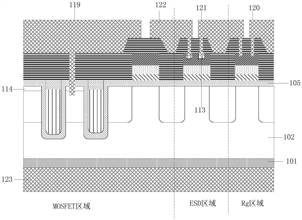
[0053] figure 1 It exemplarily shows a schematic structural diagram of a MOSFET device provided by an embodiment of the present invention, as figure 1 As shown, the MOSFET device mainly includes an active region trench 103, a first conductivity type drift layer 102, a first layer of a second conductivity type body region 109, a first layer of a second conductivity type body region 109, a first layer of a first a conductivity type source region 113 , and a fir...


PUM


Abstract

The invention discloses an MOSFET (Metal-Oxide-Semiconductor Field Effect Transistor) device and a preparation method, and relates to the field of semiconductor power devices. The anti-static and anti-impact capabilities of the grid electrode can be effectively enhanced, and the purpose of withstand voltage of the device is achieved by using the ESD polycrystalline silicon layer as a mask plate to block the injection of the P-type body region at the periphery. The method comprises the steps that active region grooves are formed in a first conduction type drift layer, a second layer of first conduction type source regions are arranged between the active region grooves and on one sides of the active region grooves, and the active region grooves are located in an MOSFET region; a first layer of second conductive type body region is arranged on the non-doped polycrystalline silicon layer in the MOSFET region; the non-doped polycrystalline silicon layer is arranged above the first conductive type drift layer; a first layer of second conductive type body region and a first layer of first conductive type source region are arranged on the non-doped polycrystalline silicon layer in the ESD region; a first layer of second conductive type body region is arranged on the non-doped polycrystalline silicon layer in the Rg region; and a second layer of second conductive type body region is arranged in the first conductive type drift layer.

Description

technical field [0001] The invention relates to the technical field of semiconductor power devices, in particular to a MOSFET device and a preparation method. Background technique [0002] For power devices MOSFE (English: Metal-Oxide-Semiconductor Field-Effect Transistor, Chinese: Metal-Oxide-Semiconductor Field-Effect Transistor) devices, in order to pursue lower internal resistance in some application fields, mainly by reducing each key size The width of the device can be achieved by increasing the device cell density, but the reduction of the critical size of the device will inevitably compress the thickness of the gate oxide layer, thereby reducing the antistatic and impact resistance of the device gate. Contents of the invention [0003] The embodiment of the present invention provides a MOSFET device and a preparation method, which can effectively enhance the antistatic and impact resistance of the gate, and use the ESD polysilicon layer as a mask to block the impla...

Claims


Application Information

Patent Timeline
IPC IPC(8): H01L29/78H01L29/423H01L29/06H01L21/336
CPCH01L29/063H01L29/7823H01L29/66704H01L29/4236
Inventor 袁力鹏唐呈前杨科完颜文娟常虹
Owner 华羿微电子股份有限公司
Why Eureka
Try Eureka